Transmission electron microscope in-situ nano indentation method for micron alloy containing isometric single nano-twin crystal

A technology of nano-twinning and transmission electron microscopy, which is applied in the use of radiation for material analysis, etc., can solve the problems that the in-situ nano-indentation method of transmission electron microscopy is difficult to implement, difficult to operate, and difficult to obtain.

Inactive Publication Date: 2018-01-23
DALIAN UNIV OF TECH
View PDF10 Cites 10 Cited by
  • Summary
  • Abstract
  • Description
  • Claims
  • Application Information

AI Technical Summary

Problems solved by technology

Due to the limitations of in-situ mechanical testing methods and instruments of transmission electron microscopy, the length and height of the test sample are required to be several microns, and contain single nanotwins of equal length. This kind of sample is difficult to obtain from the current four methods
[0004] TEM in situ nanomechanics is an effective method to study the nanoscale deformation of nanotwins, but the current research methods mainly focus on the stretching, compression and bending of elemental elements, and there are few reports on in situ nanomechanics of alloys.
[0005] TEM nanoindentation usually uses a needle tip with a radius of curvature of tens of nanometers to indent a sample with a thickness of nanometer scale. If the sample is thick, the electron beam cannot be transmitted, and the sample is thin. It is difficult for the nanoscale diamond tip to press into the sample, and When operating, the line of sight is perpendicular to the direction of pressing, so the operation is extremely difficult
TEM in situ nanoindentation method leading to microalloys containing single nanotwins of equal length is difficult to achieve

Method used


Image

  • Transmission electron microscope in-situ nano indentation method for micron alloy containing isometric single nano-twin crystal
  • Transmission electron microscope in-situ nano indentation method for micron alloy containing isometric single nano-twin crystal
  • Transmission electron microscope in-situ nano indentation method for micron alloy containing isometric single nano-twin crystal

Examples


Embodiment Construction

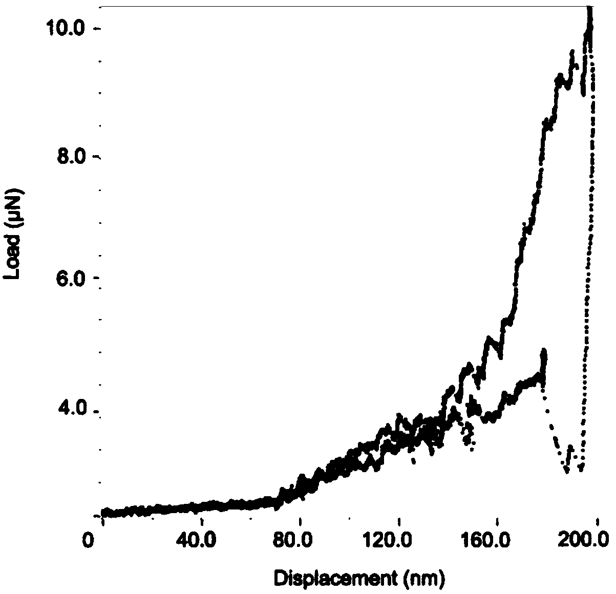
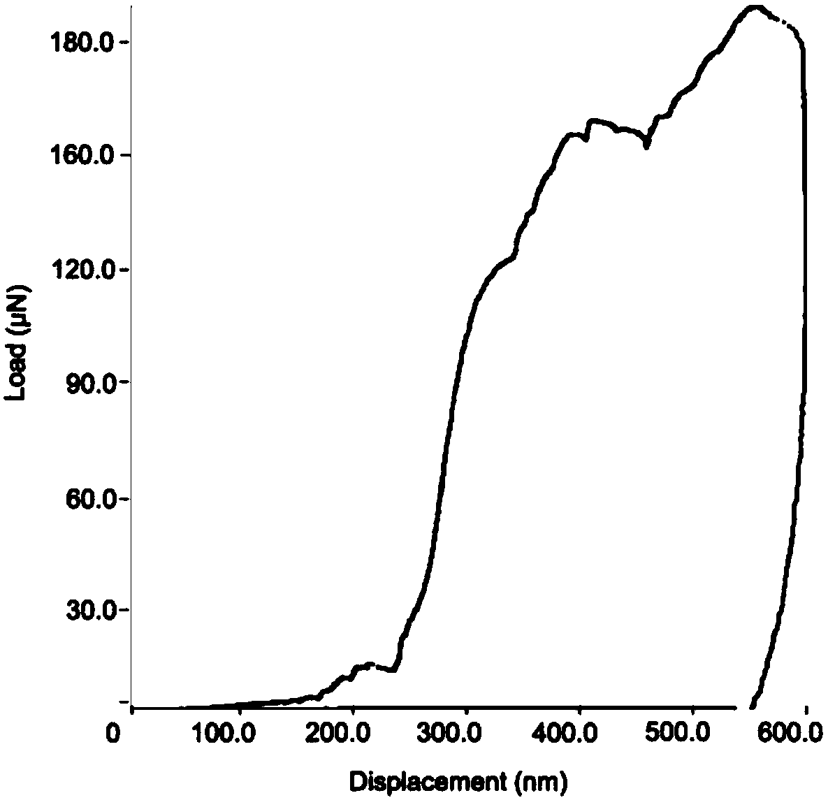
[0033] The specific implementation manner of the present invention will be described in detail below in combination with the technical scheme and accompanying drawings.

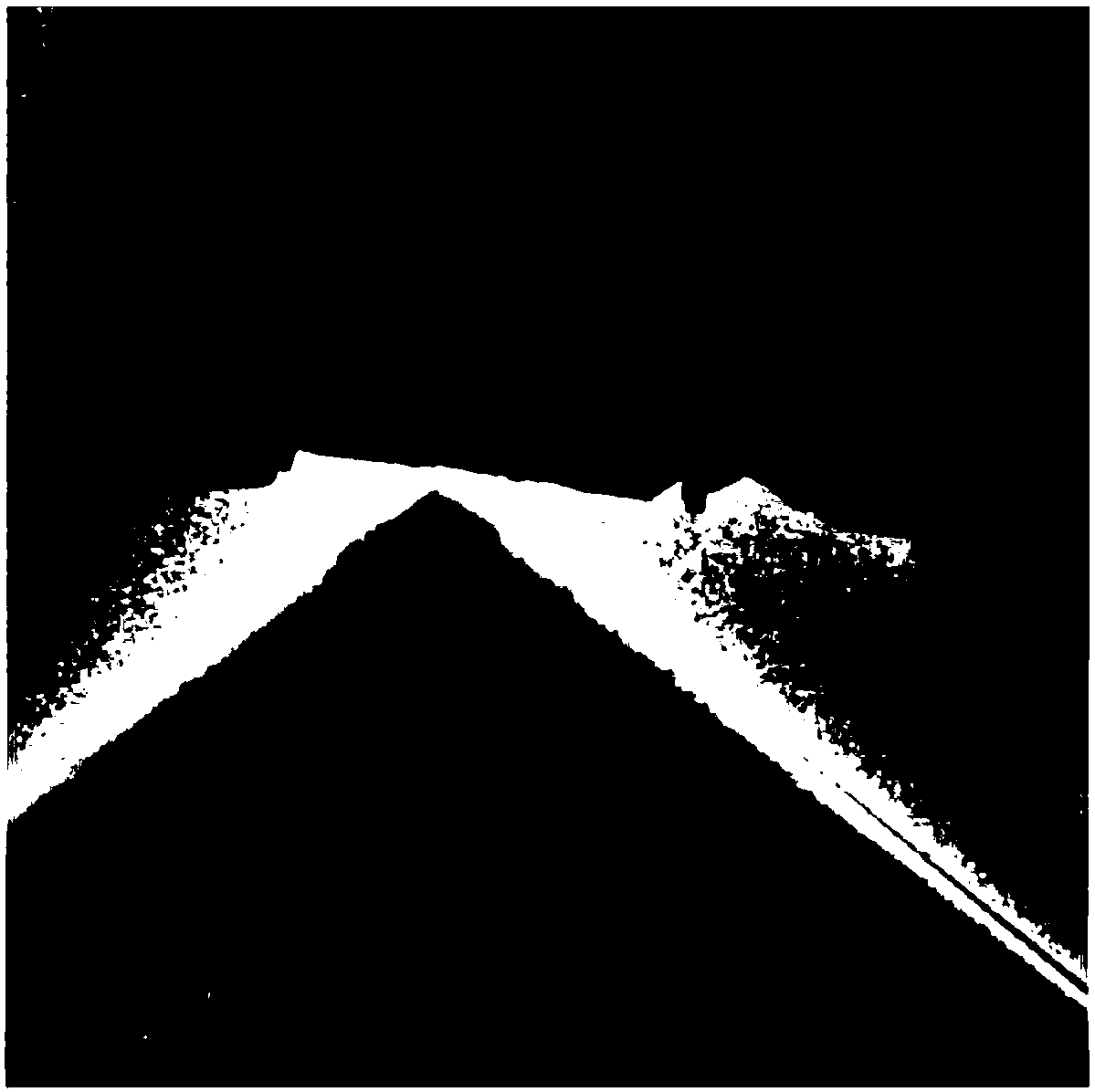
[0034] A commercial 4-inch Si(111) silicon wafer that has been chemically mechanically polished uses the Ar ion beam etching method in the IC manufacturing process to etch a quadrangular pyramid pit on the silicon wafer. The pit depth is 100-200 μm, two four The distance between the pyramids is 300-400 μm, and an array of such micro-pits is formed covering the surface of the silicon wafer. After the etching is completed, use a diamond pen to cut small pieces with a length and width of 8-9 mm. Put 4 small pieces into the chemical vapor deposition equipment to grow the macro-micro-nano integrated diamond tool. After the growth is completed, the radius of curvature of each tip is 60-90nm, and the height of the tip is 100-200μm , the distance between the tool tips is 300-400μm, the tool tips form an array, coveri...


PUM

PropertyMeasurementUnit
surface roughnessaaaaaaaaaa
lengthaaaaaaaaaa
heightaaaaaaaaaa

Abstract

The invention provides a transmission electron microscope in-situ nano indentation method for micron alloy containing isometric single nano-twin crystal, and belongs to the field of transmission electron microscope in-situ mechanical testing f nano-twin crystal. A macro-micro-nano integrated diamond tool is used, each tip has a curvature radius of 40-90 nm and a height of 100-300 Mu m; the tips are arrayed and are distributed on the surface of the tool. The diamond tool is used to indent the surface of the alloy; the indented surface is processed by chemical mechanical polishing; the polishedalloy has surface roughness Ra of 0.5-0.9 nm. A scanning electron microscope with focusing ion beams is used to perform in-situ cutting, splicing, transporting and ion thinning, and a sample has a length of 5-20 Mu m, a height of 4-10 Mu m and a thickness of 50-100 nm. A displacement control mode is used, maximum displacement is 200-1000 nm, and loading speed is 10-30 nm/s. The transmission electron microscope in-situ nano indentation method for single nano-twin crystal is achieved herein.

Description

technical field [0001] The invention belongs to the technical field of in-situ mechanical testing of transmission electron microscopy, relates to the field of in-situ mechanical testing of nanomaterials, in particular to the field of in-situ nano-indentation testing of nano-twinned transmission electron microscopy, and specifically provides a micron alloy containing a single nanometer of equal length. Twinned in situ nanoindentation method for transmission electron microscopy. Background technique [0002] In 2004, "Science" reported that the tensile strength of nano-twinned copper is 10 times that of coarse-grained copper, and maintains plasticity and electrical properties, followed by "Science" in 2009, and "Nature" in 2010 reported the highest nano-twinned copper Tensile strength, "Nature" reported nano-twinned cubic boron nitride and nano-twinned diamond in 2013 and 2014. Therefore, nano-twinned materials have become an international frontier and research hotspot in the...

Claims


Application Information

Patent Timeline
Patent Type & Authority Applications(China)
IPC IPC(8): G01N23/04
Inventor 张振宇王博崔俊峰郭东明
Owner DALIAN UNIV OF TECH
Why Eureka
Try Eureka