Method of manufacturing ZnO strip waveguide by carbon ion beam irradiation

A carbon ion beam, strip waveguide technology, applied in the direction of optical waveguide light guide, etc., can solve the problems of difficult optical waveguide structure and so on

Inactive Publication Date: 2018-01-23
TIANJIN POLYTECHNIC UNIV
View PDF5 Cites 0 Cited by
  • Summary
  • Abstract
  • Description
  • Claims
  • Application Information

AI Technical Summary

Problems solved by technology

It is difficult to realize optical waveguide structure on ZnO single crystal by high temperature diffusion, ion exchange and other methods

Method used


Image

  • Method of manufacturing ZnO strip waveguide by carbon ion beam irradiation
  • Method of manufacturing ZnO strip waveguide by carbon ion beam irradiation
  • Method of manufacturing ZnO strip waveguide by carbon ion beam irradiation

Examples


Embodiment 1

[0015] Fabrication of ZnO Ridge Optical Waveguide

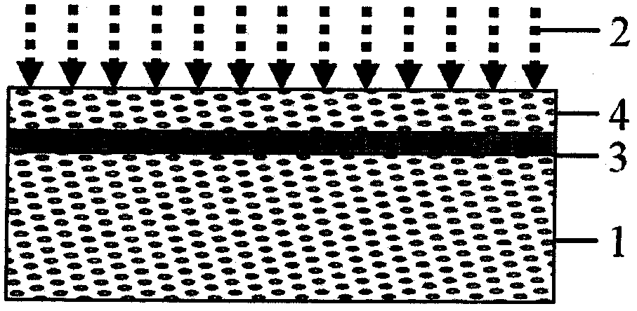
[0016] Preparation of planar waveguide: cut ZnO crystal (1) z-cut, size 5 mm×10 mm, thickness 0.5 mm, surface and end face optically polished. The ZnO crystal is cleaned with acetone, ethanol and deionized water; the prepared sample is placed in the accelerator target chamber, irradiated, the beam current is 55 nanoamperes, the energy is 4.5 MeV, and the dose is 2×10 15 ion / carbon ion per square centimeter (2), a barrier layer (3) with reduced refractive index is formed at the end of the ion beam under the crystal surface, and a planar waveguide (4) is formed between the layer and the air.

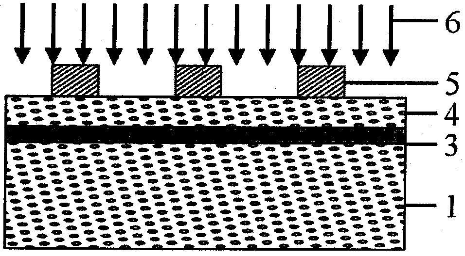
[0017] Preparation of surface mask: apply photoresist (5) on the polished surface of ZnO crystal with a high-speed coater, rotate at 3500 rpm, and bake at 80 degrees Celsius for 20 minutes. The photoresist is BP218 UV positive resist. Expose the photoresist with a photoresist plate, the photoresist plate is a 50mm×10mm chrome plate, the ...

Embodiment 2

[0021] Fabrication of ZnO Channel-Shaped Optical Waveguide

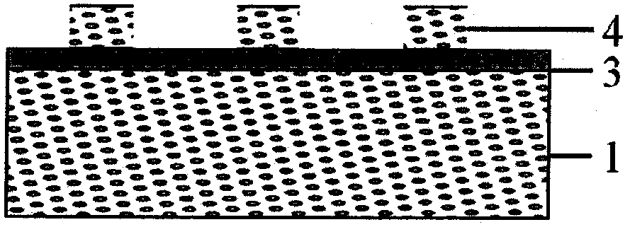
[0022] Sample polishing: cut ZnO crystal (1) z-cut, size 5 mm × 10 mm, thickness 0.5 mm, surface and end faces optically polished. After cleaning the ZnO crystals with acetone, ethanol, and deionized water, prepare the mask.

[0023] Preparation of surface mask: apply photoresist (5) on the polished surface of ZnO crystal with a high-speed coater, rotate at 3500 rpm, and bake at 80 degrees Celsius for 20 minutes. The photoresist is BP218 UV positive resist. Expose the photoresist with a photoresist plate, the photoresist plate is a 50mm×10mm chrome plate, the line shading part is 5mm, the non-shielding part is 45mm, and the stripe period is 50 microns. After exposure, develop with a special developing solution and rinse with deionized water to form a photoresist mask. The stencil produced after photolithography is heated to 160 degrees Celsius for 20 minutes under the protection of nitrogen. During this process, th...


PUM


Abstract

The invention discloses a method of manufacturing a ZnO strip optical waveguide by a combination of carbon ion beam irradiation and lithography, which belongs to the technical field of optoelectronicdevice manufacturing. Optical polishing is carried out on the surface and two end surfaces of single crystal ZnO, a strip mask is manufactured on the surface of a sample, carbon ion beam irradiation is then carried out, a photoresist mask is cleaned, and a channel strip optical waveguide is obtained; or, carbon ion beam irradiation is firstly used, the photoresist mask is then made, an Ar ion beamis then used for etching, and a rib optical waveguide is obtained. The formed strip optical waveguide can well keep the optical features of the ZnO crystal and has a hidden application value in aspects of manufacturing of an optical switch and an optical modulator.

Description

technical field [0001] The invention relates to a method for preparing single crystal optical waveguide, which is suitable for preparing ZnO strip optical waveguide by carbon ion beam irradiation. The invention relates to a waveguide preparation method belonging to the field of optoelectronic devices. technical background [0002] As the basic unit of integrated optics, optical waveguide is also the basis of all-optical network. Optical waveguide plays an important role in the manufacture of various optical devices due to its unique performance, high integration and low cost of mass production. Optical waveguides can confine light beams to a smaller area to increase optical density, thereby making better use of the optical properties of crystals or reducing the pumping threshold of optical materials, which are of great value for optical signal transmission, amplification, and modulation. A planar light guide is one in which light is constrained in one direction, while a str...

Claims


Application Information

Patent Timeline
IPC IPC(8): G02B6/13
Inventor 明宪兵张艺
Owner TIANJIN POLYTECHNIC UNIV
Why Eureka
Try Eureka