A double-sided isomer micronozzle and its manufacturing method
A technology of double-sided isomerism and manufacturing method, which is applied in rayon manufacturing, hollow filament manufacturing, textile and paper making, etc. It can solve the problems of hollow structure falling off, spinneret damage, distance narrowing, etc., and achieves good consistency , the effect of wide application field and controllable length
- Summary
- Abstract
- Description
- Claims
- Application Information
AI Technical Summary
Problems solved by technology
Method used
Image
Examples
Embodiment 1
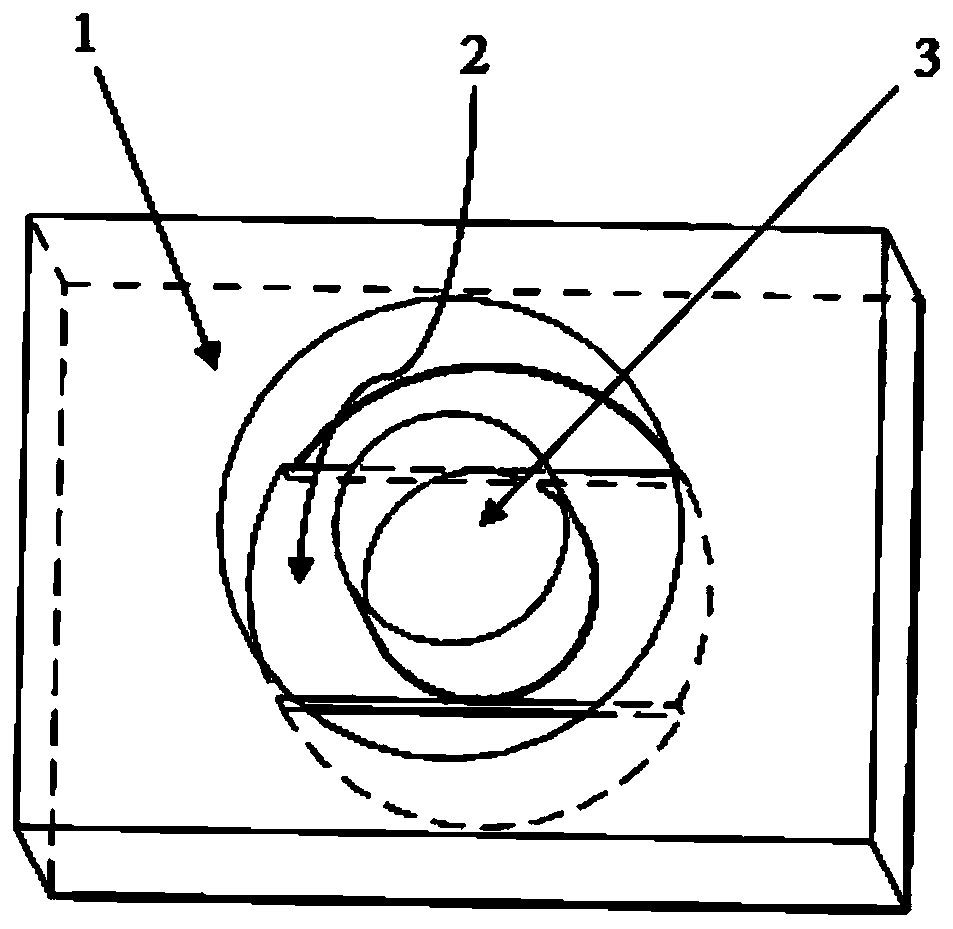
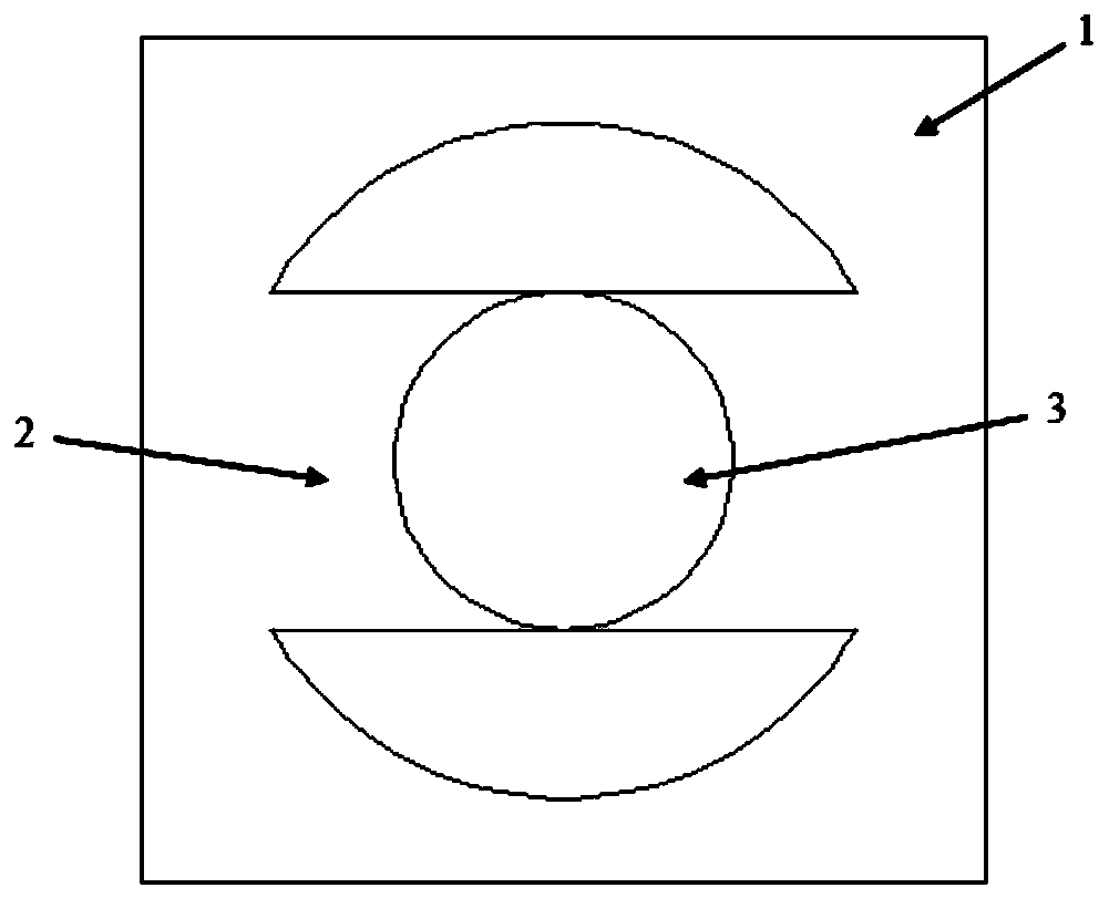
[0080] Such as figure 1 , 2 , 3, 4, and 5, this embodiment provides a method for manufacturing functional silicon-based micro-nano nozzles with heterogeneous multi-layer complex structures, which has the ability to manufacture micro-nozzles with island structures.
[0081] This method uses MEMS processing technology to manufacture micro-nozzles with special-shaped island structures (triangular, square, Y-shaped, etc. arbitrary shapes). The island structure is due to the double-sided overlay + silicon deep etching process, which can prepare a completely closed ring. As a result, the island 3 of the micro-nozzle is placed on a cantilever beam 2, and there is no connection between the island 3 and its surroundings, and it is a completely closed annular hole. According to needs, the island can be located in the center or eccentric position of the nozzle; as shown in the figure, 2 is a cantilever beam, which is a bridge composed of two semicircular holes, and 3 is a completely ind...
Embodiment 2
[0101] Such as Figure 5 , 6 As shown, this example provides another method for manufacturing double-sided isomer shaped micro-nozzles with one side being Y-shaped and one side being round. Y-shaped holes and round holes are etched on the front and back sides, which are commonly used in various graphics.
[0102] The specific steps of the method include:
[0103] (1) Draw the hole plan of Y-shaped and circular holes respectively, and make a mask plate with precise alignment symbols according to the plan;
[0104] (2) on the first side of the silicon wafer, i.e., the front side, carry out glue rejection and glue drying;
[0105] (3) on the ultraviolet exposure machine, the photoresist layer on the first side (front side) on the silicon wafer 4 is carried out ultraviolet exposure;
[0106] (4) Use a developer to develop a Y shape to protect the parts that do not need to be etched;
[0107] (5) Using an etching method to carve out a Y-shaped hole 5 on the silicon wafer 4 for...
Embodiment 3
[0115] This embodiment provides a method for manufacturing a nozzle with a multilayer composite structure, and the specific steps of the method include:
[0116] (1) The manufacturing method of double-sided special-shaped through holes is as described in embodiment 1 and embodiment 2, and will not be repeated here;
[0117] (2) Obtained by laser ablation Figure 7 The third layer of cylindrical holes;
[0118] (3) Carry out gold sputtering treatment to the surface of required bond and form a gold film on the surface of the silicon wafer;
[0119] (4) Align the silicon wafers that need to be bonded face to face, hole to hole, and fix the two silicon wafers;
[0120] (5) Put the fixed two silicon wafers into a high-temperature furnace to bond and fuse them together. So far, the silicon-gold bonding is completed. If it is a silicon-silicon bond, just skip the third and fourth steps. .
[0121] (6) According to the requirements of multi-layer structure design, multiple double-...
PUM
 Abstract
Description
Claims
Application Information


