A method for forming deep via holes
A deep through-hole, one-part technology, applied in the field of back-illuminated image sensors, can solve problems such as impact and yield loss, and achieve the effects of optimizing process, increasing yield, and reducing etching process time
- Summary
- Abstract
- Description
- Claims
- Application Information
AI Technical Summary
Problems solved by technology
Method used
Image
Examples
Embodiment Construction
[0033] It should be noted that, in the case of no conflict, the following technical solutions and technical features can be combined with each other.
[0034] The specific embodiment of the present invention will be further described below in conjunction with accompanying drawing:
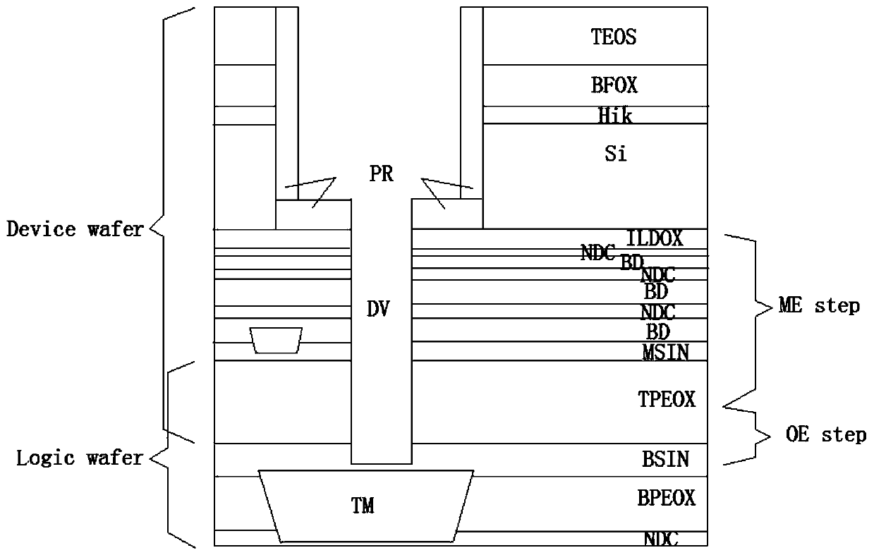
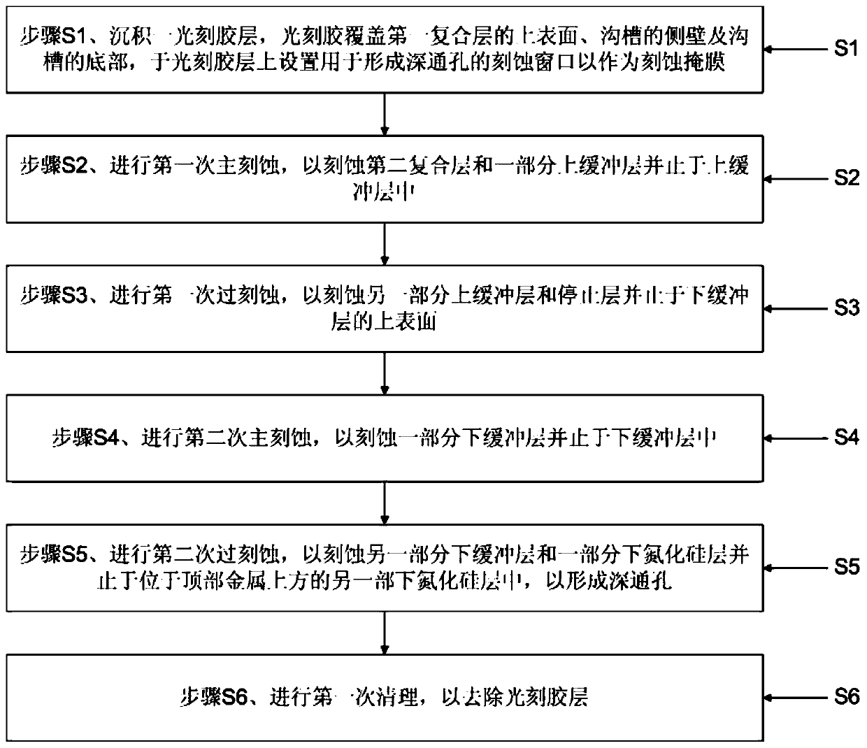
[0035] Such as Figure 3-4 As shown, a method for forming a deep through hole is suitable for a composite structure. The composite structure is formed by bonding a device wafer and a signal operation wafer. The device wafer includes a first composite layer, a The second composite layer, the middle silicon nitride layer and the buffer layer, the above-mentioned signal operation chip includes the above-mentioned buffer layer, the lower silicon nitride layer and the third composite layer arranged in sequence from top to bottom, and a trench, the bottom of the trench exposes the upper surface of the second composite layer, a top layer of metal is provided in the lower silicon nitride layer and the thi...
PUM
 Abstract
Description
Claims
Application Information


