Titanium dioxide nanorod film with high photocatalysis efficiency and preparation method thereof
A technology of titanium dioxide and nanorods, which is applied in the field of semiconductor photocatalysis, can solve the problem of large deposition area and achieve the effects of uniform film formation, uniform shape and size, and easy operation
- Summary
- Abstract
- Description
- Claims
- Application Information
AI Technical Summary
Problems solved by technology
Method used
Image
Examples
Embodiment 1
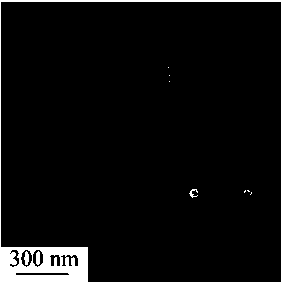
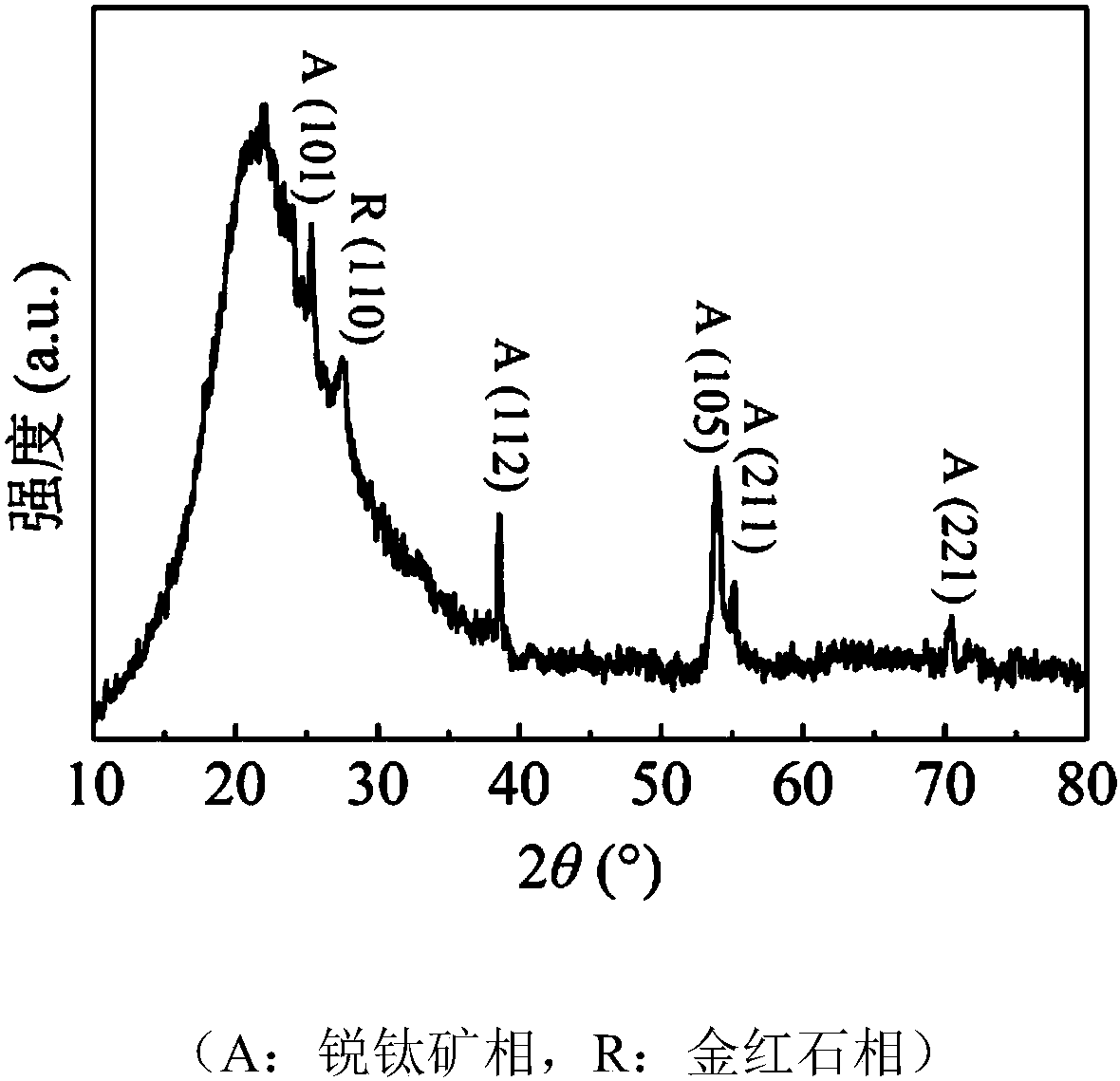
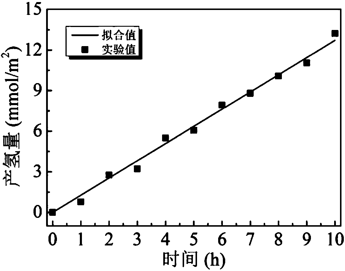
[0072] Use quartz glass as the substrate, put it into the cavity of the magnetron sputtering equipment after cleaning, and adjust the distance between the target and the substrate to 110mm. Using a mechanical pump, the molecular pump is evacuated until the cavity vacuum reaches 3.0×10 -3 After Pa, the substrate was heat-treated at 400°C for 2h. Then close the substrate baffle, feed argon gas with a flow rate of 40 sccm, adjust the sputtering power of the titanium target to 130W, the total working pressure to 0.5Pa, and pre-sputter for 30min. Afterwards, oxygen was introduced, the flow rate was 4 sccm, and the working pressure was adjusted at 0.3 Pa. The substrate baffle was opened, and the deposition of titanium dioxide nanorod film was started. The whole deposition process lasted 4 hours and the temperature of the substrate was kept at 450°C. figure 1 and figure 2 are the cross-sectional SEM and XRD patterns of the titanium dioxide film, respectively. The thickness of the...
Embodiment 2
[0074] Use quartz glass as the substrate, put it into the cavity of the magnetron sputtering equipment after cleaning, and adjust the distance between the target and the substrate to 110mm. Using a mechanical pump, the molecular pump is evacuated until the cavity vacuum reaches 4.0×10 -3 After Pa, the substrate was heat-treated at 400°C for 2h. Then close the substrate baffle, feed argon gas with a flow rate of 50 sccm, adjust the sputtering power of the titanium target to 120W, the total working pressure to 0.5Pa, and pre-sputter for 30min. Afterwards, oxygen was introduced, the flow rate was 8 sccm, and the working pressure was adjusted at 0.4Pa. The substrate baffle was opened, and the deposition of titanium dioxide nanorod film was started. The whole deposition process lasted 9 hours and the temperature of the substrate was kept at 400°C. Figure 4 are the cross-sectional SEM images of the titanium dioxide film, respectively. The titanium dioxide film thickness of gained...
Embodiment 3
[0076] Use quartz glass as the substrate, put it into the cavity of the magnetron sputtering equipment after cleaning, and adjust the distance between the target and the substrate to 110mm. Using a mechanical pump, the molecular pump is evacuated until the cavity vacuum reaches 4.0×10 -3 After Pa, the substrate was heat-treated at 400°C for 2h. Then close the substrate baffle, feed argon gas with a flow rate of 30 sccm, adjust the sputtering power of the titanium target to 100W, the total working pressure to 0.5Pa, and pre-sputter for 30min. Afterwards, oxygen was introduced at a flow rate of 15 sccm, and the working pressure was adjusted at 0.5 Pa. The substrate baffle was opened to start the deposition of the titanium dioxide nanorod film. The entire deposition process lasted 20 hours and the temperature of the substrate was kept at 500°C. Figure 6 and Figure 7 are the cross-sectional SEM and XRD patterns of the titanium dioxide film, respectively. The obtained titanium...
PUM
| Property | Measurement | Unit |
|---|---|---|
| thickness | aaaaa | aaaaa |
| thickness | aaaaa | aaaaa |
| thickness | aaaaa | aaaaa |
Abstract
Description
Claims
Application Information
 - R&D
- Intellectual Property
- Life Sciences
- Materials
- Tech Scout
- Unparalleled Data Quality
- Higher Quality Content
- 60% Fewer Hallucinations
Browse by: Latest US Patents, China's latest patents, Technical Efficacy Thesaurus, Application Domain, Technology Topic, Popular Technical Reports.
© 2025 PatSnap. All rights reserved.Legal|Privacy policy|Modern Slavery Act Transparency Statement|Sitemap|About US| Contact US: help@patsnap.com


