Perovskite solar cell taking graphdiyne-induced crosslinking fullerene in-plane orientation as electron transmission layer and preparation method of perovskite solar cell
An electron transport layer and solar cell technology, applied in the field of solar cells, can solve problems such as harsh preparation conditions, achieve the effects of simplifying the preparation process, avoiding degradation reactions, and improving electron mobility
- Summary
- Abstract
- Description
- Claims
- Application Information
AI Technical Summary
Problems solved by technology
Method used
Image
Examples
Embodiment 1
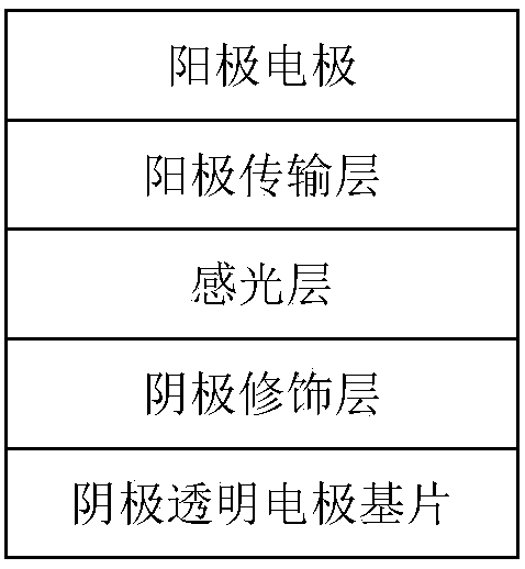
[0030] A two-dimensional graphyne-induced cross-linked fullerene in-plane orientation as a perovskite solar cell with a highly conductive electron transport layer, the preparation steps of the preparation method are as follows:
[0031] (1) Dissolve 180mg of methylammonium iodide and 553mg of lead iodide in a mixed solvent of γ-butyrolactone and dimethyl sulfoxide (volume ratio 7:3), and stir for 5 hours to make 40wt% calcium Titanium solution;
[0032] (2) Dissolve and disperse 1 mg of the highly conductive two-dimensional material graphyne and 20 mg of the compound PCBSD in 1 mL of chlorobenzene, spin-coat it on the FTO glass substrate at a speed of 4000 rpm for 40 s, and then anneal at 140 ° C to form a thickness of 45 nm. The cured cathodic modification layer;
[0033] (3) Spin-coat the perovskite γ-butyrolactone and dimethyl sulfoxide solution obtained in (1) on the cathode modification layer obtained in (2) at a speed of 4000 rpm for 40 seconds, and then Lower annealin...
Embodiment 2
[0037] A two-dimensional graphyne-induced cross-linked fullerene in-plane orientation as a perovskite solar cell with a highly conductive electron transport layer, the preparation steps of the preparation method are as follows:
[0038] (1) Dissolve 180mg of methylammonium iodide and 553mg of lead iodide in a mixed solvent of γ-butyrolactone and dimethyl sulfoxide (volume ratio 7:3), and stir for 5 hours to make 40wt% calcium Titanium solution;
[0039] (2) The titanium dioxide precursor solution was spin-coated on the FTO glass substrate at a rotation speed of 4000rpm for 40s, and then annealed at 500°C to form a cured cathode modification layer with a thickness of 45nm;
[0040] (3) Dissolve 1 mg of highly conductive two-dimensional material graphyne and 20 mg of compound PCBSD in 1 mL of chlorobenzene, spin-coat it on titanium dioxide at a speed of 4000 rpm for 40 s, and then anneal at 140 ° C to form a solidified layer with a thickness of 20 nm. The cathode modification l...
Embodiment 3
[0045] A two-dimensional graphyne-induced cross-linked fullerene in-plane orientation as a perovskite solar cell with a highly conductive electron transport layer, the preparation steps of the preparation method are as follows:
[0046] (1) Dissolve 180mg of methylammonium iodide and 553mg of lead iodide in a mixed solvent of γ-butyrolactone and dimethyl sulfoxide (volume ratio 7:3), and stir for 5 hours to make 40wt% calcium Titanium solution;
[0047] (2) Dissolve and disperse 1 mg of the highly conductive two-dimensional material graphyne and 20 mg of the compound PCBSD in 1 mL of chlorobenzene, spin-coat it on a flexible ITO substrate at a speed of 4000 rpm for 40 s, and then anneal at 80 ° C to form a thickness of 45 nm. The cured cathodic modification layer;
[0048] (3) Spin-coat the perovskite γ-butyrolactone and dimethyl sulfoxide solution obtained in (1) on the cathode modification layer obtained in (2) at a speed of 4000 rpm for 40 seconds, and then Lower annealin...
PUM
| Property | Measurement | Unit |
|---|---|---|
| Thickness | aaaaa | aaaaa |
| Thickness | aaaaa | aaaaa |
| Thickness | aaaaa | aaaaa |
Abstract
Description
Claims
Application Information

