Trench gate charge storage type insulated gate bipolar transistor and manufacturing method therefor

A bipolar transistor and charge storage technology, which is applied in semiconductor/solid-state device manufacturing, circuits, electrical components, etc., can solve the problems of increasing device saturation current density, increasing device switching loss, and increasing switching loss

Active Publication Date: 2018-03-13
UNIV OF ELECTRONICS SCI & TECH OF CHINA
View PDF5 Cites 30 Cited by
  • Summary
  • Abstract
  • Description
  • Claims
  • Application Information

AI Technical Summary

Problems solved by technology

[0005] The implementation of method (1) will increase the gate-emitter capacitance and gate-collector capacitance at the same time, and the switching process of the IGBT is essentially the process of charging / discharging the gate capacitance, so the increase in the gate capacitance will Makes the charging / discharging time longer, which in turn causes the switching speed to decrease
Therefore, the deep trench gate depth will reduce the switching speed of the device, increase the switching loss of the device, and affect the compromise characteristics of the device's conduction voltage drop and switching loss; and the implementation of method (2) will increase the device's switching loss The gate capacitance will reduce the switching speed of the device and increase the switching loss, which will affect the compromise between the conduction voltage drop and switching loss of the device. On the other hand, the large channel density will also increase the saturation current density of the device, making the device short-circuit safe. work area deterioration
In addition, the gate oxide layer in the trench gate structure is formed in the trench by one thermal oxidation. In order to ensure a certain threshold voltage, the thickness of the entire gate oxide layer is required to be small. However, the MOS capacitance and the thickness of the oxide layer Inversely proportional, which makes the thin gate oxide thickness in traditional CSTBT devices will significantly increase the gate capacitance of the device, and the electric field concentration effect at the bottom of the trench will reduce the breakdown voltage of the device, resulting in poor reliability of the device

Method used


Image

  • Trench gate charge storage type insulated gate bipolar transistor and manufacturing method therefor
  • Trench gate charge storage type insulated gate bipolar transistor and manufacturing method therefor
  • Trench gate charge storage type insulated gate bipolar transistor and manufacturing method therefor

Examples


Embodiment 1

[0078] This example proposes as figure 2 A trench gate charge storage type insulated gate bipolar transistor is shown, and its cell structure includes: a P-type collector region 12, a collector metal 13 located on the back of the P-type collector region 12, a collector metal 13 located on the back of the P-type collector region The N-type electric field stop layer 11 on the front side of the region 12 and the N-type drift region 10 above the N-type electric field stop layer 11; the N-type drift region 10 has an N+ emitter region 3, a P+ emitter region 4, a P-type base region 5, and an N-type drift region 10. type charge storage layer 6, P-type body region 71 and trench gate structure; the trench gate structure partially penetrates the N-type drift region 10 along the vertical direction of the device; the P-type body region 71 is located on one side of the trench gate structure, and the P-type The base region 5 is located on the other side of the trench gate structure, and the...

Embodiment 2

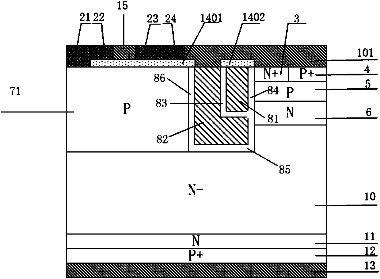
[0080] This implementation proposes as image 3A trench gate charge storage type insulated gate bipolar transistor is shown, with a P-type collector region 12, a collector metal 13 located on the back of the P-type collector region 12, and an N-type electrode located on the front side of the P-type collector region 12. The electric field stop layer 11 and the N-type drift region 10 located above the N-type electric field stop layer 11; the N-type drift region 10 has an N+ emitter region 3, a P+ emitter region 4, a P-type base region 5, an N-type charge storage layer 6, The P-type body region 71 and the trench gate structure; the trench gate structure partially penetrates the N-type drift region 10 along the vertical direction; the P-type body region 71 is located on one side of the trench gate structure, and the P-type base region 5 is located at the trench gate The other side of the structure, and the junction depth of the P-type body region 71 is greater than the junction de...

Embodiment 3

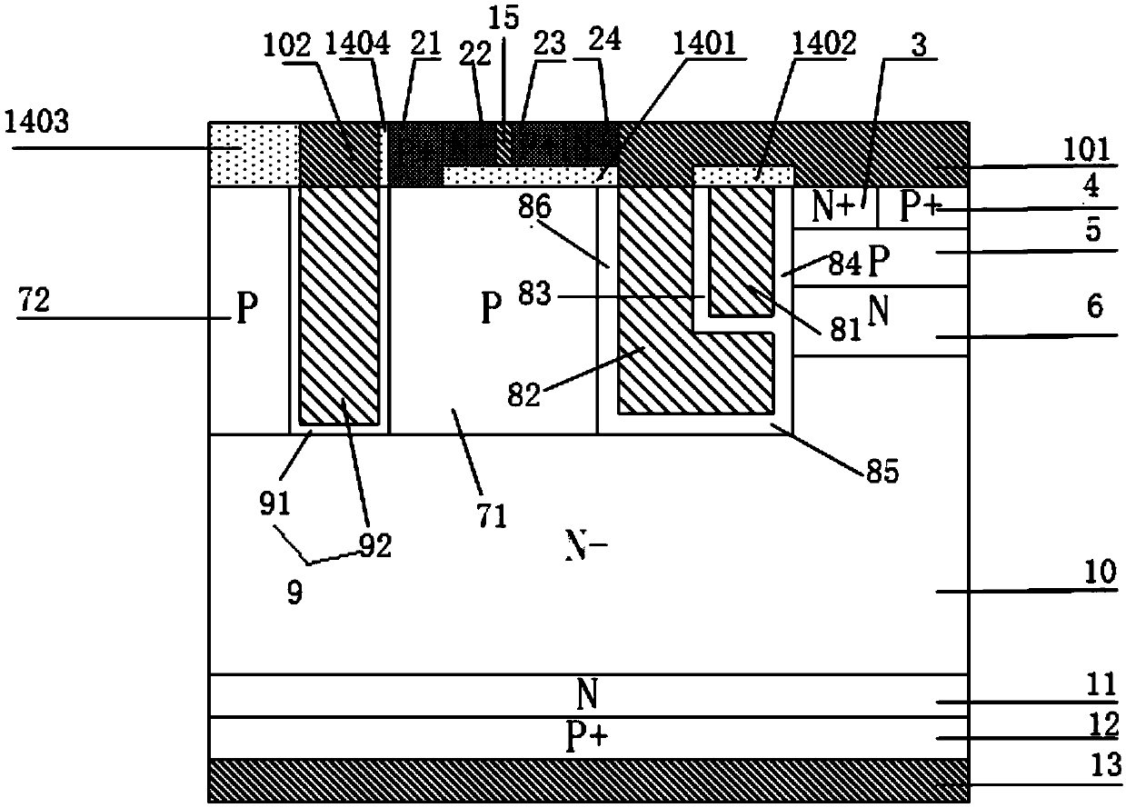
[0083] This example proposes a Figure 4 In the shown trench gate charge storage type insulated gate bipolar transistor, in this embodiment, the thickness of the split electrode dielectric layer (that is, the first split electrode dielectric layer 85 and the second split electrode dielectric layer 86) is greater than that of the gate dielectric layer (that is, the thicknesses of the first gate dielectric layer 83 and the second gate dielectric layer 84 ), the rest are the same as those in Embodiment 2.

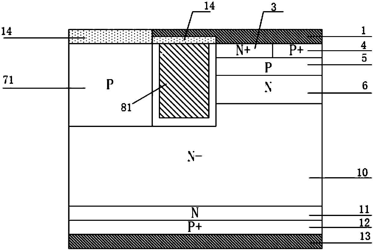
[0084] Such as figure 1 Shown is the structure of a traditional trench gate charge storage type insulated gate bipolar transistor. The gate oxide layer is formed in the trench by one thermal oxidation. In order to ensure a certain threshold voltage, the thickness of the entire gate oxide layer is small. The MOS capacitance is inversely proportional to the thickness of the gate oxide layer. Therefore, the thin gate oxide layer thickness in the traditional CSTBT structure great...


PUM


Abstract

The invention discloses a trench gate charge storage type insulated gate bipolar transistor and a manufacturing method therefor, and belongs to the technical field of a semiconductor power device. Byovercoming the adverse influence of an N type charge storage layer in the conventional structure, more excellent voltage withstand performance is obtained; and compared with the conventional mode, thecompromising characteristic among the switching performance, switch-on voltage drop and switching loss of the device is realized by increasing the trench gate depth and reducing cellular width, and the problem of reliability degradation is solved. By introducing a series diode structure into a P type body region, the channel voltage of an MOSFET is clamped at a quite small value, thereby loweringdevice saturated current density and improving the short-circuit safety working region of the device; by introducing a split electrode and a split electrode dielectric layer to the trench gate structure, the threshold voltage and switching speed of the device are ensured while the switching performance of the device is improved; and by virtue of the floating P type body region, the compromising characteristic between the forward switch-on voltage drop and switching loss of the device is improved. In addition, the manufacturing process of the CSTBT device is compatible with the conventional manufacturing process.

Description

technical field [0001] The invention belongs to the technical field of semiconductor power devices, in particular to an insulated gate bipolar transistor (IGBT), in particular to a trench gate charge storage type insulated gate bipolar transistor (CSTBT). Background technique [0002] Insulated gate bipolar transistor (IGBT), as one of the core electronic components in modern power electronic circuits, is widely used in various fields such as transportation, communication, household appliances, and aerospace. Insulated gate bipolar transistor (IGBT) is a new type of power electronic device composed of an insulated field effect transistor (MOSFET) and a bipolar junction transistor (BJT), which can be equivalent to a MOSFET driven by a bipolar junction transistor. . IGBT combines the working mechanism of MOSFET structure and bipolar junction transistor. It not only has the advantages of MOSFET easy to drive, low input impedance, and fast switching speed, but also has the adva...

Claims


Application Information

Patent Timeline
Patent Type & Authority Applications(China)
IPC IPC(8): H01L29/06H01L29/423H01L29/739H01L21/331
CPCH01L29/0607H01L29/42312H01L29/66325H01L29/7393
Inventor 张金平赵倩刘竞秀李泽宏任敏张波
Owner UNIV OF ELECTRONICS SCI & TECH OF CHINA
Why Eureka
Try Eureka