Preparation method, product and application of tungsten oxide electron transfer layer
A technology of electron transport layer and tungsten oxide, which is applied in the direction of final product manufacturing, circuit, photovoltaic power generation, etc., can solve the problems of few reports, achieve the effect of wide adjustable range of parameters, simple process and process, and strong repeatability
- Summary
- Abstract
- Description
- Claims
- Application Information
AI Technical Summary
Problems solved by technology
Method used
Image
Examples
Embodiment 1
[0033] (1) Measure 5ml of n-propanol solution, weigh 0.5g of tungsten hexachloride, dissolve tungsten hexachloride in n-propanol to obtain a solubility of 0.1g / ml, stir until completely dissolved, and obtain a yellow solution ;
[0034] (2) Continue to stir, the yellow solution turns into a transparent light blue solution;
[0035] (3) Spin coating on the cleaned FTO conductive glass at a speed of 3000rmp for 30s;
[0036] (4) The spin-coated substrate is heated in an oven at 150 degrees Celsius for 15 minutes;
[0037] (5) In order to obtain better film quality, repeat the above steps (3) and (4) 3 times to obtain a tungsten oxide electron transport layer material with stable performance;
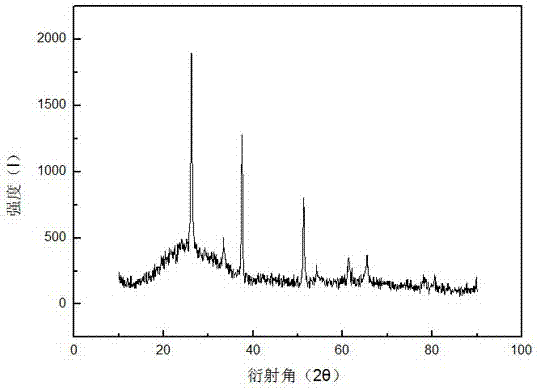
[0038] The crystal form of the tungsten oxide thin film obtained by the above preparation method is consistent with the standard powder diffraction card (JCPDS: 36-1451). On the basis of the prepared electron transport layer, the perovskite layer and the hole transport layer Spiro-OMeTA...
Embodiment 2
[0040] (1) Measure 5ml of isopropanol solution, weigh 0.25g of tungsten hexachloride, dissolve tungsten hexachloride in isopropanol to obtain a solubility of 0.05g / ml, stir until completely dissolved, and obtain a yellow solution ;
[0041] (2) Continue to stir, the yellow solution turns into a transparent light blue solution;
[0042] (3) Spin coating on the cleaned FTO conductive glass at a speed of 2500rmp for 40s;
[0043] (4) The spin-coated substrate is heated in an oven at 150 degrees Celsius for 25 minutes;
[0044] (5) In order to obtain better film quality, repeat the above steps (3) and (4) 3 times to obtain a tungsten oxide electron transport layer material with stable performance;
[0045] The crystal form of the tungsten oxide thin film obtained by the above preparation method is consistent with the standard powder diffraction card (JCPDS: 36-1451). On the basis of the prepared electron transport layer, the perovskite layer and the hole transport layer Spiro-O...
Embodiment 3
[0048] (1) Measure 5ml of n-butanol solution, weigh 0.5g of tungsten hexachloride, dissolve tungsten hexachloride in n-butanol to obtain a solubility of 0.1g / ml, stir until completely dissolved, and obtain a yellow solution ;
[0049](2) Continue to stir, the yellow solution turns into a transparent light blue solution;
[0050] (3) Spin coating on the cleaned FTO conductive glass at a speed of 3500rmp for 30s;
[0051] (4) The spin-coated substrate is heated in an oven at 150 degrees Celsius for 20 minutes;
[0052] (5) In order to obtain better film quality, repeat the above steps (3) and (4) 3 times to obtain a tungsten oxide electron transport layer material with stable performance;
[0053] The crystal form of the tungsten oxide thin film obtained by the above preparation method is consistent with the standard powder diffraction card (JCPDS: 36-1451). On the basis of the prepared electron transport layer, the perovskite layer and the hole transport layer Spiro-OMeTAD w...
PUM
 Abstract
Description
Claims
Application Information
 - R&D
- Intellectual Property
- Life Sciences
- Materials
- Tech Scout
- Unparalleled Data Quality
- Higher Quality Content
- 60% Fewer Hallucinations
Browse by: Latest US Patents, China's latest patents, Technical Efficacy Thesaurus, Application Domain, Technology Topic, Popular Technical Reports.
© 2025 PatSnap. All rights reserved.Legal|Privacy policy|Modern Slavery Act Transparency Statement|Sitemap|About US| Contact US: help@patsnap.com


