Single-side suede preparation method of crystal silicon solar cell
A technology of solar cells and crystalline silicon, applied in the field of solar cells, can solve problems such as uninvolved, many process steps, and reduce compounding on the back of silicon wafers, so as to achieve the effects of reducing production costs, improving production efficiency, and reducing chemical consumption
- Summary
- Abstract
- Description
- Claims
- Application Information
AI Technical Summary
Problems solved by technology
Method used
Image
Examples
preparation example Construction
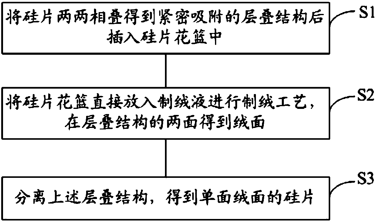
[0049] ginseng figure 1 As shown, the invention discloses a method for preparing a single-sided suede surface of a crystalline silicon solar cell, comprising the following steps:
[0050]S1. Stack the silicon wafers in pairs to obtain a tightly adsorbed laminated structure and then insert them into the silicon wafer flower basket.
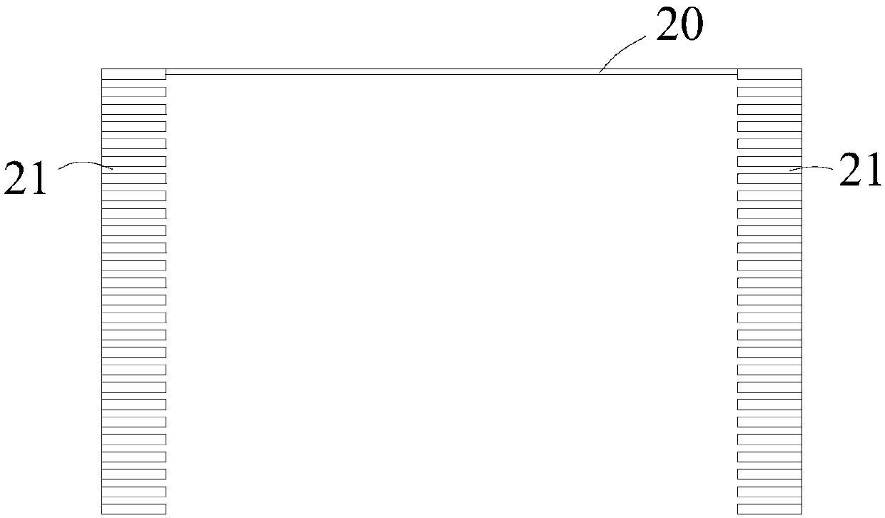
[0051] Schematic diagram of the structure of the silicon wafer flower basket 20 figure 2 As shown, it is exactly the same as the existing silicon flower basket, and the two side walls of the silicon flower basket are correspondingly provided with several slots 21. Preferably, the silicon flower basket in the present invention contains 25 correspondingly arranged slots, each Two stacked silicon chips can be inserted into each corresponding slot, and a total of 50 silicon chips can be inserted. Of course, the number of slots can be changed according to needs, for example, 50 slots can be set, and 100 silicon chips can be inserted correspondingly, ...
Embodiment 1
[0080] A method for preparing a single-sided textured surface of a crystalline silicon solar cell, comprising the steps of:
[0081] 1. Chemically etch or polish the P-type polysilicon wafers with a size of 156.75mm×156.75mm and a thickness of 180±10μm on both sides, stack 50 pieces of the above-mentioned polished silicon wafers in pairs to obtain a tightly adsorbed laminated structure, and then insert 25 pieces Standard silicon wafer flower basket for texturing;
[0082] 2. Put the flower basket of silicon wafers directly into the acidic texturing solution for the texturing process. The main steps include:
[0083] 1) Put the flower basket of silicon wafers into the 3 In the HF solution, the HF concentration is 0.1mol / L, and the Ag attachment reaction is carried out at room temperature for 30s;
[0084] 2) Put the stacked silicon wafer structure after the previous step into HF and H 2 o 2 In the mixed solution, the concentrations were 3mol / L and 0.1mol / L respectively, and...
Embodiment 2
[0091] A method for preparing a single-sided textured surface of a crystalline silicon solar cell, comprising the steps of:
[0092] 1. Chemically etch or polish the P-type monocrystalline silicon wafers with a size of 156.75mm×156.75mm and a thickness of 180±10μm on both sides, and stack 50 pieces of the above-mentioned polished silicon wafers in pairs to obtain a tightly adsorbed laminated structure. Insert 25 pieces of special silicon wafer flower basket for texturing;
[0093] 2. Put the flower basket of silicon wafers directly into the alkaline texturing liquid for the texturing process. The main steps include:
[0094] Put the flower basket of silicon wafer directly into the texturing solution to carry out the texturing process. The main steps include: putting it into the KOH solution with a concentration of 2% containing single crystal texturing additives, and reacting at 80°C for 500s;
[0095] 3. Separating the above-mentioned stacked structure to obtain a silicon wa...
PUM
| Property | Measurement | Unit |
|---|---|---|
| thickness | aaaaa | aaaaa |
Abstract
Description
Claims
Application Information


