High-precision micro-nano size two-dimensional material electrode preparation method

A two-dimensional material, high-precision technology, applied in circuits, electrical components, electrical digital data processing, etc., can solve the problems of difficult electrodes, low precision, irregular shapes, etc., to achieve accurate positioning, high precision, and wide application range. Effect

Active Publication Date: 2018-04-20
EAST CHINA NORMAL UNIV
View PDF4 Cites 3 Cited by
  • Summary
  • Abstract
  • Description
  • Claims
  • Application Information

AI Technical Summary

Problems solved by technology

It is necessary to test the electrical properties of two-dimensional materials by preparing electrodes on two-dimensional materials. However, due to the small size and irregular shape of two-dimensional materials, it is necessary to prepare electrodes on two-dimensional materials without affecting the performance of two-dimensional materials. The right electrode is a big problem
In the traditional technology, there is a method of preparing electrodes on two-dimensional materials by electron beam evaporation relying on copper mesh or other masks, but for some two-dimensional materials that cannot be transferred in a large area, it is inconvenient to control the position of two-dimensional materials, and for some The utilization rate of two-dimensional materials with a small area is low, and it is cumbersome to make a mask plate for each situation. In addition, this method is not easy to control the size of the two-dimensional materials between electrodes, and the accuracy is relatively low. Low

Method used


Image

  • High-precision micro-nano size two-dimensional material electrode preparation method
  • High-precision micro-nano size two-dimensional material electrode preparation method
  • High-precision micro-nano size two-dimensional material electrode preparation method

Examples


Embodiment 1

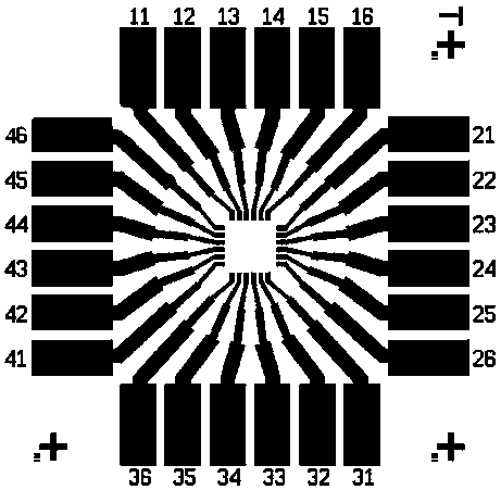
[0022] 1) Save the photolithographic layout of the preset electrodes into the computer;

[0023] 2) Molybdenum disulfide was prepared by mechanical exfoliation and then transferred to a silicon substrate with preset electrodes by adhesive tape;

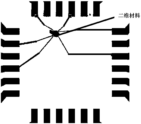
[0024] 3) Place the silicon substrate in step 2) under an optical microscope, measure the length of the molybdenum disulfide to be 15.2 microns, and the width to be 7.5 microns, and take pictures of the molybdenum disulfide and surrounding electrodes;

[0025] 4) Open the picture taken in step 3) in the image processing software, select the molybdenum disulfide and the electrode, paint red, and paint the rest white, and save it; image processing uses photoshop software;

[0026] 5) Open the picture saved in step 4) in the layout software, adjust the unit under the layout software, rotate the figure, and move the position of the figure, so that the electrode pattern in the picture overlaps with the electrode in the lithography layout o...

Embodiment 2

[0031] 1) Save the photolithographic layout of the preset electrodes into the computer;

[0032] 2) Prepare tantalum disulfide by mechanical exfoliation method and then transfer it to silicon substrate with preset electrodes through adhesive tape;

[0033] 3) Place the silicon substrate in step 2) under an optical microscope, measure the length of the tantalum disulfide to be 30.1 microns, and the width to be 5.2 microns, and take pictures of the tantalum disulfide and surrounding electrodes;

[0034] 4) Open the picture taken in step 3) in the image processing software, select the tantalum disulfide and the electrode, paint red, and paint the rest white, and save it; image processing uses photoshop software;

[0035] 5) Open the picture saved in step 4) in the layout software, adjust the unit under the layout software, rotate the figure, and move the position of the figure, so that the electrode pattern in the picture overlaps with the electrode in the lithography layout of t...

Embodiment 3

[0040] 1) Save the photolithographic layout of the preset electrodes into the computer;

[0041] 2) Prepare tungsten diselenide by mechanical stripping method and then transfer it to the silicon substrate with preset electrodes through adhesive tape;

[0042] 3) Place the silicon substrate in step 2) under an optical microscope, measure the length of tungsten diselenide to be 23 microns, and the width to be 7 microns, and take pictures of tungsten diselenide and surrounding electrodes;

[0043] 4) Open the picture taken in step 3) in the image processing software, select tungsten diselenide and the electrode, paint red, and paint the rest in white, and save it; image processing uses photoshop software;

[0044] 5) Open the picture saved in step 4) in the layout software, adjust the unit under the layout software, rotate the figure, and move the position of the figure, so that the electrode pattern in the picture overlaps with the electrode in the lithography layout of the pres...


PUM


Abstract

The invention discloses a high-precision micro-nano size two-dimensional material electrode preparation method. The high-precision micro-nano size two-dimensional material electrode preparation methodcomprises the steps of: transferring a two-dimensional material to a silicon substrate provided with a preset electrode; subjecting the silicon substrate to observation and photographing under a microscope; performing image processing on a photographed image on image processing software; opening the processed image in layout software, and drawing electrodes as required; and preparing the electrodes by means of electron beam exposure. The high-precision micro-nano size two-dimensional material electrode preparation method is low in cost and high in efficiency, draws different electrode patterns on the layout processing software according to different requirements, efficiently controls the size and shape of the electrodes, and is wide in application range.

Description

technical field [0001] The invention belongs to the fields of material science and electronic science and technology, and in particular relates to an efficient and controllable high-precision micro-nano size two-dimensional material electrode preparation method. Background technique [0002] In the past 10 years, the research field of two-dimensional materials has attracted much attention. Because of its excellent electrical, mechanical, thermal, optical and other properties, especially electrical properties, researchers believe that it is expected to replace traditional silicon-based devices. It is necessary to test the electrical properties of two-dimensional materials by preparing electrodes on two-dimensional materials. However, due to the small size and irregular shape of two-dimensional materials, it is necessary to prepare electrodes on two-dimensional materials without affecting the performance of two-dimensional materials. A suitable electrode is a big problem. In ...

Claims


Application Information

Patent Timeline
Patent Type & Authority Applications(China)
IPC IPC(8): H01L21/28G06F17/50G06T11/40
CPCG06F30/20G06T11/40H01L21/28
Inventor 吴幸夏银徐何军
Owner EAST CHINA NORMAL UNIV
Why Eureka
Try Eureka