Carrier storage layer IGBT device with shielding gates

A technology of carrier storage and shielding gate, applied in semiconductor devices, electrical components, circuits, etc., can solve the problems of reducing the switching speed of the device, increasing the saturation current density of the device, reducing the breakdown voltage of the device, etc., to reduce the switching loss. , Improve the effect of switching speed

Inactive Publication Date: 2018-05-04
UNIV OF ELECTRONICS SCI & TECH OF CHINA
View PDF2 Cites 6 Cited by
  • Summary
  • Abstract
  • Description
  • Claims
  • Application Information

AI Technical Summary

Problems solved by technology

However, for CSTBT devices, the newly added N-type carrier storage layer with high concentration and certain thickness makes the breakdown voltage of the device significantly lower
Therefore, in order to effectively shield the negative impact of the N-type carrier storage layer on the device withstand voltage, two methods are generally adopted: 1. Increase the depth of the trench, which means that the depth of the trench gate is greater than that of the N-type carrier storage layer. Deep; 2. Reduce the width of the cell, so that the distance between the trench gates is as small as possible; however, these two methods will make the gate-emitter capacitance (Cge) and gate-collector capacitance (Cgc) of the device significantly increase
On the one hand, a large capacitance reduces the switching speed of the device, increases the switching loss of the device, and affects the compromise between the forward conduction voltage drop and switching loss of the device. On the other hand, it increases the saturation current density of the device, making the device The breaking characteristics of the circuit become worse

Method used


Image

  • Carrier storage layer IGBT device with shielding gates
  • Carrier storage layer IGBT device with shielding gates
  • Carrier storage layer IGBT device with shielding gates

Examples


Embodiment 1

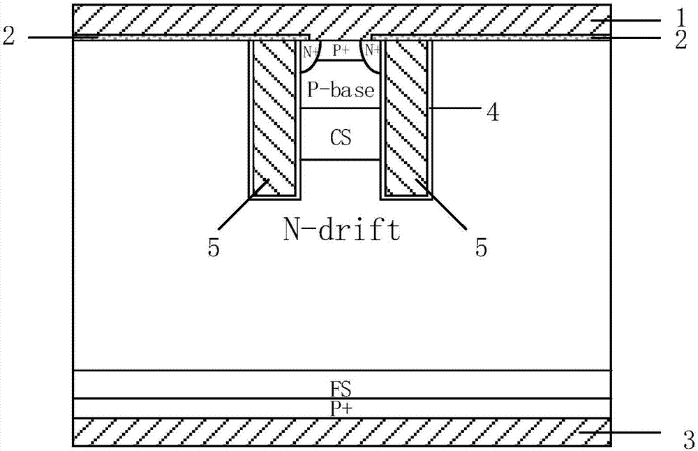
[0025] Such as figure 2 As shown, a carrier storage layer IGBT device with a shielded gate, including a collector metal 3, a first conductivity type semiconductor collector P+, a second conductivity type semiconductor field stop region FS, The second conductivity type semiconductor drift region N-drift, inside the second conductivity type semiconductor drift region N-drift is provided with a trench gate structure, the second conductivity type semiconductor carrier storage region CS, and the first conductivity type semiconductor base region P- Base, the second conductivity type semiconductor emitter region N+, the first conductivity type semiconductor emitter region P+, the emitter metal 1 is arranged above the second conductivity type semiconductor drift region N-drift; the trench gate structure includes two left and right control Gate 4 and two left and right shielding gates 5, and the control gate structure 4 and shielding gate structure 5 penetrate the second conductivity ...

Embodiment 2

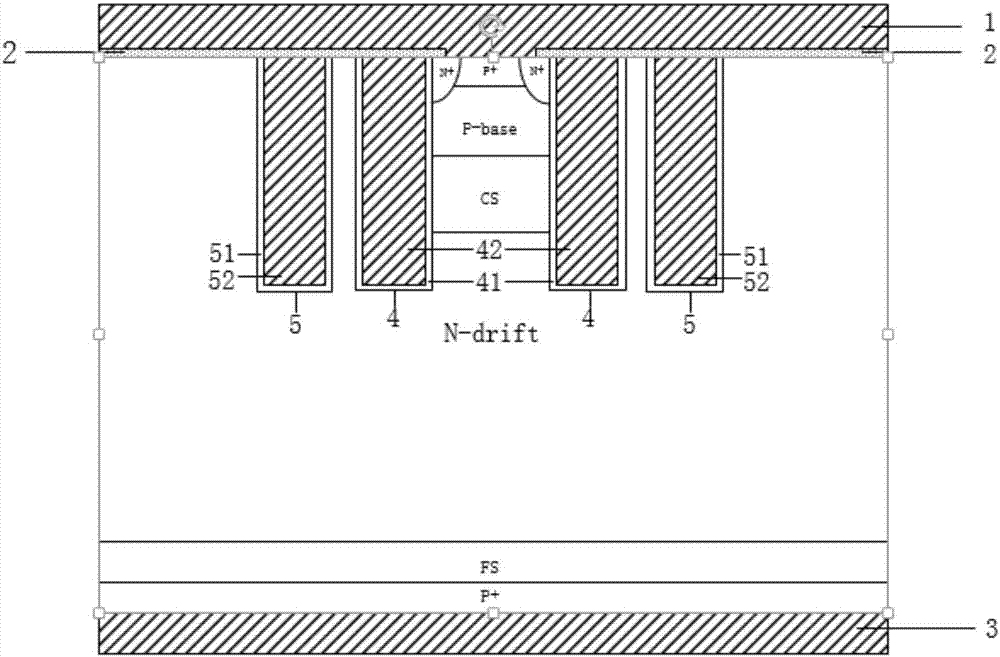
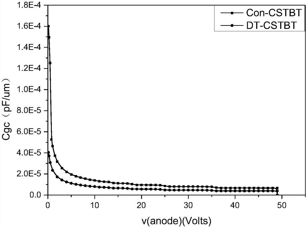
[0037] Such as Figure 5 As shown, a carrier storage layer IGBT device with a shielding gate in this embodiment differs from Embodiment 1 in that the depth of the shielding gate 5 is deeper than that of the control gate 4 . The effect of the shielding gate on reducing the gate-emitter capacitance (Cge) and the gate-collector capacitance (Cgc) is better.


PUM


Abstract

The invention provides a carrier storage layer IGBT (insulated gate bipolar transistor) device with shielding gates. According to the invention, under the condition that the cell width of the device is kept at a certain value, the distance between trench gates is reduced by adding a floating shielding gate on the two sides of an original trench gate. Meanwhile, the grid-emitter capacitance and thegrid-collector capacitance of the device are also reduced, and the switching speed of the device is increased. The switching loss is reduced. Meanwhile, the saturation current density of the device is reduced, so that the short-circuit working area is improved. The voltage-withstanding performance of the device is improved. By reasonably adjusting the concentration thickness of the carrier storage area and the distance between shielding gates, the grid-emitter capacitance and the grid-collector capacitance of the device are reduced under the condition that the breakdown voltage is the same asthat of a conventional carrier storage trench bipolar transistor. As a result, the effect of improving the switching speed is achieved.

Description

technical field [0001] The invention belongs to the technical field of power devices, and relates to an insulated gate bipolar transistor (IGBT), in particular to a trench gate carrier storage type insulated gate bipolar transistor (CSTBT). Background technique [0002] In recent years, with the rapid development of microelectronics technology, society has continuously increased the requirements for the most advantageous power devices in electronic power, and the advantages of insulated gate bipolar transistors, one of the representatives of power devices, have attracted widespread attention. Insulated Gate Bipolar Transistor (IGBT) is a new type of power electronic device combining MOS field effect and bipolar transistor. It not only has the advantages of easy driving and simple control of MOSFET, but also has the advantages of low conduction voltage of power transistor, large on-state current and small loss. It has become one of the core electronic components in modern pow...

Claims


Application Information

Patent Timeline
Patent Type & Authority Applications(China)
IPC IPC(8): H01L29/739H01L29/423
CPCH01L29/4236H01L29/7397
Inventor 李泽宏殷鹏飞彭鑫赵倩任敏张金平高巍张波
Owner UNIV OF ELECTRONICS SCI & TECH OF CHINA
Why Eureka
Try Eureka