Wafer-level package structure and package process applied to acoustic surface wave filter

A wafer-level packaging, surface acoustic wave technology, applied in electrical components, impedance networks, etc., can solve the problems of low processing efficiency, low efficiency, increase bonding force, etc., to improve processing efficiency, improve processing efficiency, and improve reliability. sexual effect

Active Publication Date: 2018-05-08
CHINA ELECTRONICS TECH GRP CORP CHONGQING ACOUSTIC OPTIC ELECTRONICS CO LTD
View PDF7 Cites 9 Cited by
  • Summary
  • Abstract
  • Description
  • Claims
  • Application Information

AI Technical Summary

Problems solved by technology

There are two reasons for the large size: First, the diameter of the metal solder ball (gold or tin ball) connected between the chip and the substrate is generally not less than 80um, and a large amount of space needs to be flowed around the solder ball as a margin, which is a lot of waste The chip area is increased; secondly, the bonding force between the organic film used for gas sealing and the substrate is relatively poor, and a large area (200um) around the substrate needs to be occupied to increase the bonding force
[0006] 2. High material cost
If tin balls are used, the volume can be reduced, but the electroplating process will generate a large amount of waste water containing lead, which will pollute the environment and cost a lot of treatment.
If gold balls are used, expensive high-purity gold is required, which is very expensive
3) A special gas-sealed organic film is required to complete the sealing of the device, which is not only costly, but also requires a large substrate area
[0007] 3. Low processing efficiency
Although the above process has improved in terms of device volume and cost, there are still some deficiencies: 1. Due to the

Method used


Image

  • Wafer-level package structure and package process applied to acoustic surface wave filter

Examples


Embodiment Construction

[0027] The present invention will be described in detail below in conjunction with the accompanying drawings and specific embodiments.

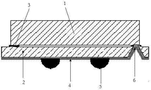
[0028] see figure 1 , it can be seen from the figure that the present invention is applied to the wafer-level packaging structure of the surface acoustic wave filter, including the filter chip substrate 1 (the commonly used material is lithium tantalate) and the packaging wafer 2, in the filter chip A circle of gold film 3 is plated on the periphery of the working surface of the substrate 1, and a circle of gold film 3 is also plated on the package wafer 2 corresponding to the gold film of each chip substrate, and the filter chip substrate 1 and the package wafer 2 pass through gold-gold bonding. An external circuit wiring structure 4 and metal solder balls 5 (usually gold balls or tin balls) for electrical connection with the PCB board are provided on the side of the packaging wafer 2 facing away from the working surface of the chip. The t...


PUM


Abstract

The invention discloses a wafer-level package structure and package process applied to an acoustic surface wave filter. The wafer-level package structure comprises a filter chip substrate and a package wafer; a circle of gold film is plated on the periphery of a working face of the filter chip substrate, and a circle of gold film is respectively plated on the position, corresponding to each chip substrate gold film, of the package wafer; the filter chip and the package wafer are combined together through a gold-gold binding way; an external circuit wiring structure and a metal solder ball electrically connected with a PCB board are arranged on the surface, reverse to the chip working face, of the packaging wafer; a through hole is formed in the package wafer to enable the chip working facecircuit to electrically connect with the metal solder ball after passing through the through hole and the external circuit wiring structure in order. The package wafer is the glass material with thethermal expansion coefficient same or approximate to that of the chip substrate material. The package disclosed by the invention is more reliable, capable of improving the efficiency and easy to eliminate the thermal mismatch condition of the device.

Description

technical field [0001] The invention relates to a surface acoustic wave filter, in particular to a wafer-level packaging structure and a packaging process applied to a surface acoustic wave filter, and belongs to the technical field of surface acoustic wave filter packaging. Background technique [0002] Do not directly contact the working surface of the surface acoustic wave filter chip with air or moisture, which will cause corrosion or oxidation on the working surface and affect the performance of the device. Therefore, in actual processing, the working surface of the chip needs to be packaged to protect it. After packaging Then connect with the PCB board. [0003] Existing SAW filters are mainly packaged by flip-chip soldering (CSP) technology. The basic principle of CSP packaging is very simple. First, metal solder balls (gold or tin) are grown on the wafer forming the chip by ultrasonic welding or reflow soldering process, then cut into individual chips, and then flip...

Claims


Application Information

Patent Timeline
IPC IPC(8): H03H9/02H03H9/64
CPCH03H9/02543H03H9/02622H03H9/64
Inventor 金中何西良杜雪松
Owner CHINA ELECTRONICS TECH GRP CORP CHONGQING ACOUSTIC OPTIC ELECTRONICS CO LTD
Why Eureka
Try Eureka