Perovskite phototransistor and fabrication method thereof

A phototransistor and perovskite technology, applied in the field of photodetectors, can solve the problems of deterioration of IGZO material characteristics, large dark current of phototransistor, etc., and achieve the effects of fast generation speed, reduced dark current and high mobility

Pending Publication Date: 2018-05-11
PEKING UNIV SHENZHEN GRADUATE SCHOOL
View PDF0 Cites 8 Cited by
  • Summary
  • Abstract
  • Description
  • Claims
  • Application Information

AI Technical Summary

Problems solved by technology

[0003] In the process of realizing the present invention, the inventors found that there are at least the following problems in the prior art: the organic-inorganic hybrid perovskite material is in direct contact with the metal oxide, and the ions of the perovskite material enter the metal oxide represented by IGZO In the layer, the deterioration of IGZO material characteristics is caused; the dark current of the phototransistor is large

Method used


Image

  • Perovskite phototransistor and fabrication method thereof
  • Perovskite phototransistor and fabrication method thereof
  • Perovskite phototransistor and fabrication method thereof

Examples


preparation example Construction

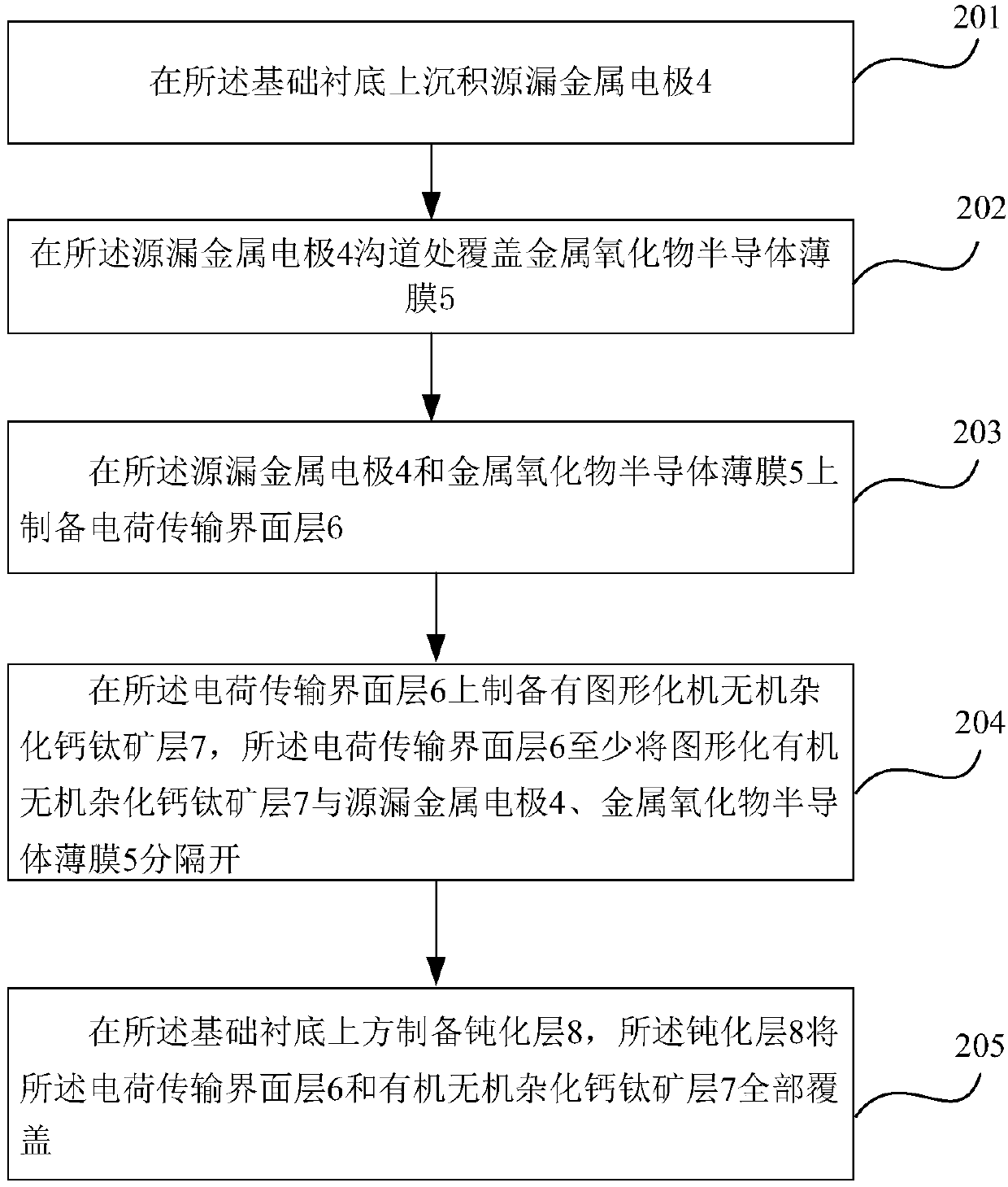
[0053] Corresponding to the above method embodiment, such as image 3 As shown, it is a flow chart of the method for preparing a perovskite phototransistor according to an embodiment of the present invention, and the method includes:

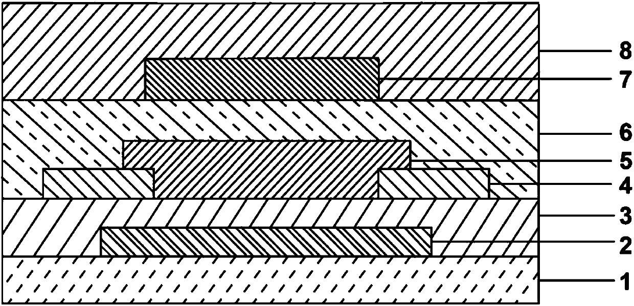
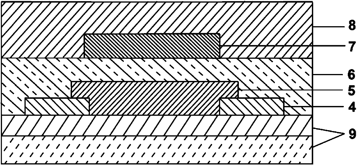
[0054] 201. Deposit source-drain metal electrodes 4 on the base substrate; please also refer to Figure 7 and Figure 11 , Figure 7 It is a schematic diagram of the structure after depositing the source-drain metal electrode 4 in Example 1 of the present invention, Figure 11 It is a schematic diagram of the structure of the source-drain metal electrode 4 deposited on the silicon substrate 9 covered with silicon dioxide in Example 2 of the present invention; Both ends of the upper surface of the base substrate, such as Figure 7 Shown: the drain metal electrode 4 is on the gate insulating layer 3, such as Figure 11 Shown: the drain metal electrode 4 is on a silicon substrate 9 covered with silicon dioxide.

[0055] 202. Cover the metal o...


PUM

PropertyMeasurementUnit
thicknessaaaaaaaaaa
thicknessaaaaaaaaaa
thicknessaaaaaaaaaa

Abstract

The embodiment of the invention provides a perovskite phototransistor and a fabrication method thereof, and belongs to the field of optical detection. The phototransistor device comprises a basic substrate, a drain-source metal electrode and a metal oxide semiconductor thin film, wherein the drain-source metal electrode is arranged on the basic substrate, a charge transmission interface layer covers the metal oxide semiconductor thin film, a patterned organic-inorganic hybrid perovskite material layer is arranged above the charge transmission interface layer, the patterned organic-inorganic hybrid perovskite material layer is at least separated from the source-drain metal electrode and the metal oxide thin film by the charge transmission interface layer, and a passivation layer is arrangedabove the basic substrate and completely covers the device. The perovskite phototransistor is of a bottom-grid bottom-contact structure and has the characteristics of low dark current, fast responsespeed and wide spectrum response; and compared with a silicon-based photoelectric detector, the perovskite phototransistor has the characteristics of low cost and low preparation energy consumption, and the device fabrication process is favorably compatible with a current silicon-based process platform.

Description

technical field [0001] The invention relates to the field of photodetectors, in particular to a perovskite phototransistor device and a preparation method thereof. Background technique [0002] Metal oxide semiconductor thin film transistors, especially indium gallium zinc oxide (IGZO) thin film transistors have the characteristics of stability, high mobility, transparency, and good uniformity, and are widely used in display panel arrays and detector arrays, but IGZO materials are due to Its forbidden band width is relatively large (>3eV), and it has no obvious response to the visible light band above 420nm. Organic-inorganic hybrid perovskite materials have the characteristics of wide light absorption range, high carrier mobility, fast carrier generation speed, long carrier diffusion length, and long carrier lifetime. Organic-inorganic hybrid calcium The excellent light absorption characteristics of titanium ore materials make it widely used in the field of photodetecto...

Claims


Application Information

Patent Timeline
Patent Type & Authority Applications(China)
IPC IPC(8): H01L51/42H01L51/48
CPCH10K30/10H10K30/65H10K30/00Y02E10/549Y02P70/50
Inventor 周航许晓特张盛东
Owner PEKING UNIV SHENZHEN GRADUATE SCHOOL
Why Eureka
Try Eureka