
Double-frequency broadband microwave sensor

A microwave sensor and broadband technology, which is applied in the field of dual-frequency broadband microwave sensors, can solve the problems of increasing the difficulty and cost of processing, complex de-embedding technology, and not suitable for widespread promotion, and achieve low processing difficulty, simple structure, and low price. Effect

Pending Publication Date: 2018-05-29
HENAN NORMAL UNIV
View PDF0 Cites 6 Cited by
  • Summary
  • Abstract
  • Description
  • Claims
  • Application Information

AI Technical Summary

Problems solved by technology

In the transmission / reflection method, the broadband measurement method based on the coplanar waveguide transmission line has achieved considerable development. The basic idea is to place the sample to be tested on the coplanar waveguide transmission line, and measure the scattering parameter information of the two ports combined with de-embedding technology. Or other algorithms (such as neural network algorithm) to invert the dielectric properties of the measured sample, its advantage is ultra-wideband measurement, the disadvantage is limited sensitivity, sometimes faced with complex de-embedding technology
In order to improve the test sensitivity, various methods have been proposed, the literature "Haase N M N, Fuge G, Trieu H K, et al. Miniaturized Transmission-Line Sensor for Broadband Dielectric Characterization of Biological Liquids and Cell Suspensions [J]. IEEE Transactions on Microwave Theory & Techniques, 2015, 63(10):3026-3033.” reported that the dielectric property detection of broadband liquid biological media was realized by loading microfluidic channels. The processing of microfluidic channels requires special processes, which increases the difficulty and cost of processing. Not suitable for widespread promotion

Method used

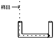
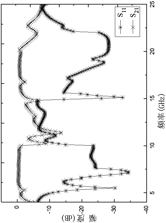

Image

  • Double-frequency broadband microwave sensor
  • Double-frequency broadband microwave sensor
  • Double-frequency broadband microwave sensor

Examples


Embodiment Construction

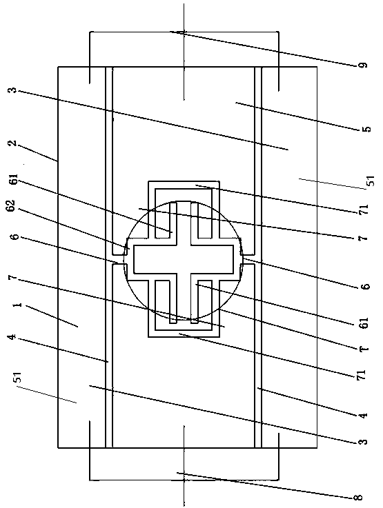
[0016] The specific content of the present invention will be described in detail in conjunction with the accompanying drawings. Such as figure 1 As shown, the sensor of the present invention is composed of a double-layer board, the bottom layer is a dielectric substrate 1, and the upper layer is a metal layer 2, and a coplanar waveguide transmission line 3 is etched on the metal layer 2, which includes two signal transmission slots 4 , the middle conduction belt 5 and the metal ground 51, the second slot line slit 6 is loaded in series on the middle conduction band 5 and away from the feeders at both ends, and the other ends of the second slot line slit 6 are respectively connected to two mutually symmetrical and identical structures. The composite branch 7 is connected, and the composite branch 7 is composed of a coplanar waveguide 71 with an open terminal and two slot line branches 61 with a short circuit at the terminal. The two composite branches 7 with the same structure ...


PUM

PropertyMeasurementUnit
Thicknessaaaaaaaaaa
Widthaaaaaaaaaa
Gap widthaaaaaaaaaa

Abstract

The invention discloses a double-frequency broadband microwave sensor. The double-frequency broadband microwave sensor comprises a coplanar waveguide transmission line, and two combined nodules whichare of the same structure and loaded on an intermediate conduction band of the coplanar waveguide transmission line in series; each combined nodule is composed of a terminal-open-circuited coplanar waveguide and two terminal-short-circuited slot line nodules which are connected with the terminal-open-circuited coplanar waveguide in parallel; the two ends of the combined nodules are connected withtwo signal transmission gaps of the coplanar waveguide transmission line in series through first slot line gaps and second slot line gaps in sequence, and the two combined nodules which are of the same structure are provided with test zones for placing to-be-tested samples. The test device is simple in structure and high in sensitivity; the slot line gaps and the combined nodules on the sensor areprocessed with a traditional etching process, the price is low, the processing difficulty is low, batch production is facilitated, and online real-time double-frequency broadband detection can be achieved.

Description

technical field [0001] The invention belongs to the technical field of dielectric constant measuring devices, in particular to a dual-frequency broadband microwave sensor. Background technique [0002] With the application of microwave technology in the fields of biology, cytology, food chemical industry and electromagnetic compatibility, many new interdisciplinary subjects have emerged, such as microwave chemistry and electromagnetic field biomedicine. However, due to insufficient research on the interaction mechanism between microwaves and biological media or chemical substances, the application of microwave technology in the above fields still faces many technical barriers. The electrical parameters of biological media or chemical substances are important parameters that reflect the interaction between microwaves and them. For example, in the field of biology, studies such as thermal denaturation of proteins, double-layered plasma membranes, single-cell characteristics, a...

Claims


Application Information

Patent Timeline
IPC IPC(8): G01N22/00
CPCG01N22/00
Inventor 刘伟娜施艳艳
Owner HENAN NORMAL UNIV
Learn More