GaAs base improved window layer structure green-yellow light LED and manufacturing method thereof
A manufacturing method and a technology for a window layer, which are applied in the field of optoelectronics, can solve the problems of no window layer improvement scheme, poor epitaxial deposition efficiency at the edge of the carrier disc, and low light efficiency, so as to ensure current expansion and optical properties, and improve external quantum Efficiency, improve the effect of product light efficiency
- Summary
- Abstract
- Description
- Claims
- Application Information
AI Technical Summary
Problems solved by technology
Method used
Image
Examples
Embodiment 1
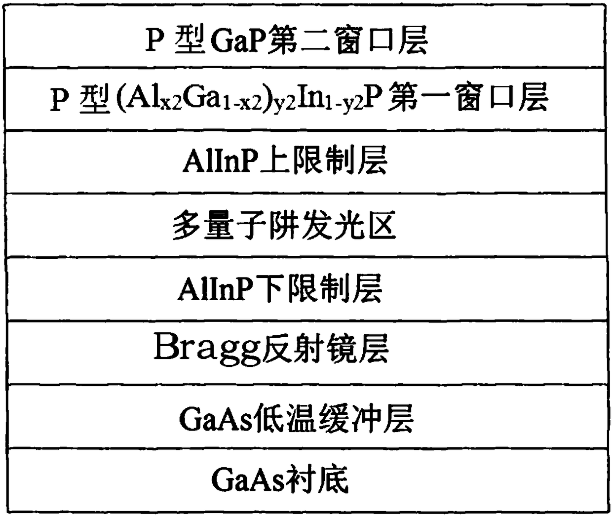
[0042] A GaAs-based yellow-green LED with an improved window layer structure, comprising a GaAs substrate, a GaAs low-temperature buffer layer, a Bragg mirror layer, an AlInP lower confinement layer, a multi-quantum well light-emitting region, an AlInP upper confinement layer, (Al x2 Ga 1-x2 ) y2 In 1-y2 a P first window layer and a P-type GaP second window layer.
Embodiment 2
[0044] A method for manufacturing a GaAs-based yellow-green LED with an improved window layer structure, comprising the following steps:
[0045] (1) Put the GaAs substrate in the growth chamber of the MOCVD equipment, H 2 The environment is heated to 800±20°C and baked for 30 minutes, and AsH is introduced 3 , removing water and oxygen on the surface of the substrate to complete the surface heat treatment to prepare for step (2);
[0046] (2) Slowly lower the temperature to 750±20°C, and continue to feed TMGa and AsH 3 , grow a GaAs low-temperature buffer layer with a thickness of 0.5um on the GaAs substrate; the cooling time is 120s;
[0047] (3) Keep the temperature at 750±20°C, and continue to feed TMGa, TMAl, and AsH 3 , growing a Bragg reflector layer on the GaAs low-temperature buffer layer in step (2), the Bragg reflector layer being AlGaAs;
[0048] (4) The temperature drops to 700±20°C, and TMIn, TMAl, and PH are introduced 3 , growing an n-type AlInP lower conf...
Embodiment 3
[0055] A method for manufacturing a GaAs-based yellow-green LED with an improved window layer structure, the steps of which are as described in Example 2, except that in step (2), the cooling time is 150s.
PUM
 Abstract
Description
Claims
Application Information
 - R&D
- Intellectual Property
- Life Sciences
- Materials
- Tech Scout
- Unparalleled Data Quality
- Higher Quality Content
- 60% Fewer Hallucinations
Browse by: Latest US Patents, China's latest patents, Technical Efficacy Thesaurus, Application Domain, Technology Topic, Popular Technical Reports.
© 2025 PatSnap. All rights reserved.Legal|Privacy policy|Modern Slavery Act Transparency Statement|Sitemap|About US| Contact US: help@patsnap.com

