Perovskite LED containing organic-inorganic hybrid perovskite monocrystal light emitting layer, and preparation method
A perovskite and light-emitting layer technology, which is applied in the direction of organic semiconductor devices, semiconductor/solid-state device manufacturing, electrical components, etc., can solve problems such as device leakage, poor device stability, and affect the stability of perovskite LEDs, and achieve layer structure Controlled, thickness-optimized results
- Summary
- Abstract
- Description
- Claims
- Application Information
AI Technical Summary
Problems solved by technology
Method used
Image

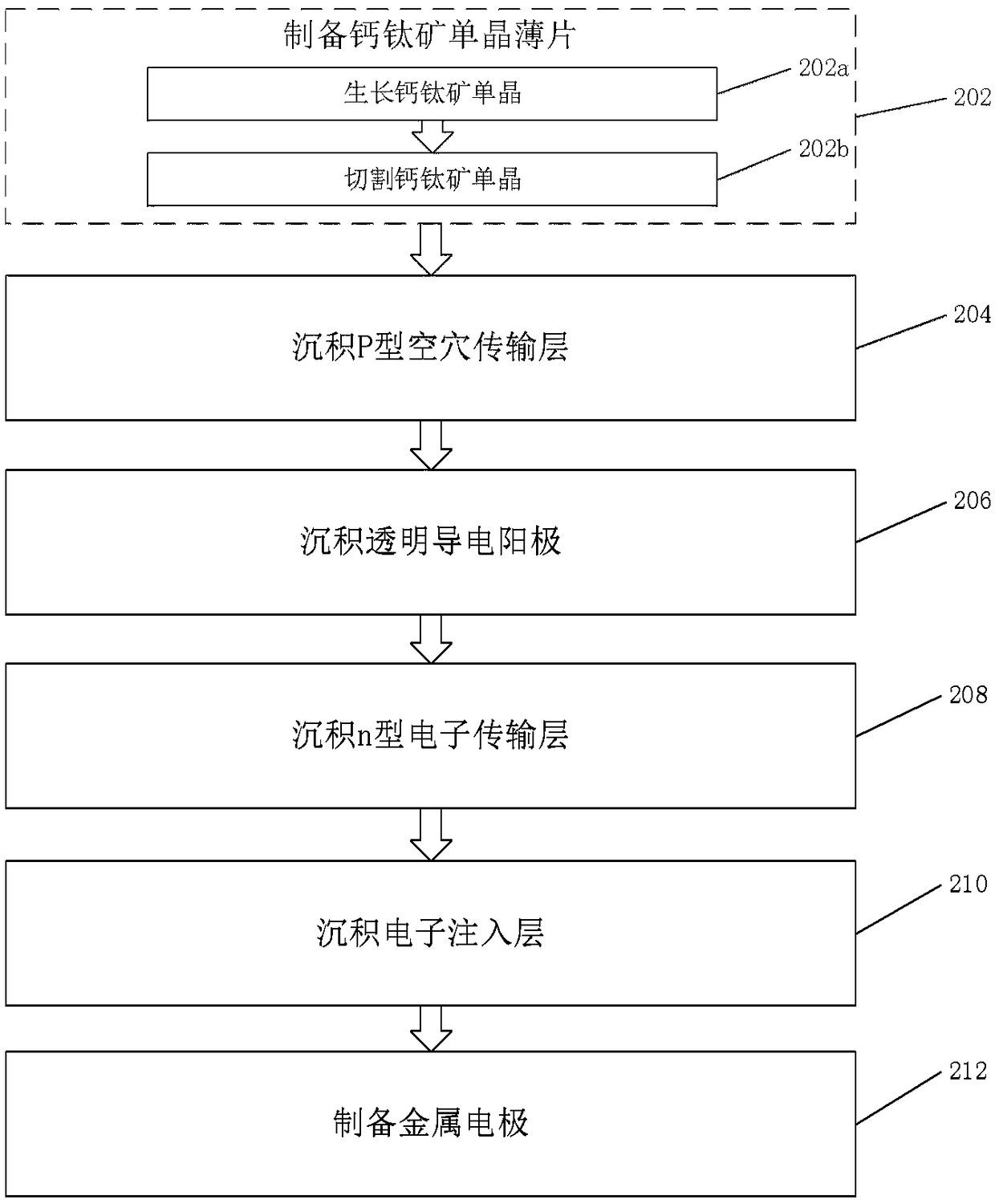
Examples
no. 1 example
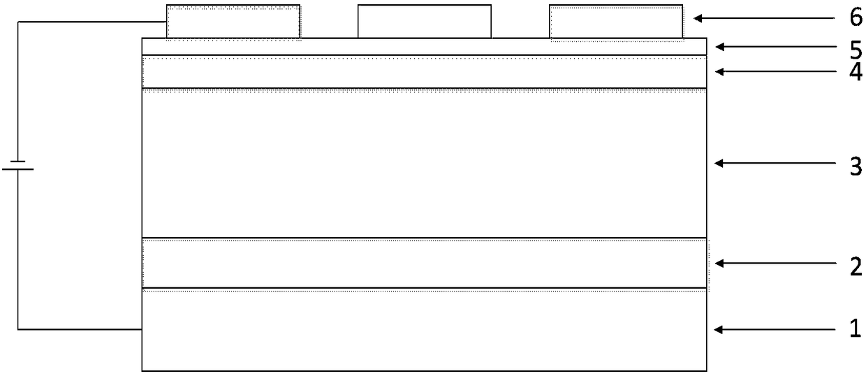
[0050] figure 1 It is a schematic structural diagram of the perovskite LED according to the first embodiment of the present disclosure. Please refer to figure 1 , the present disclosure is a perovskite LED containing an organic-inorganic hybrid perovskite single crystal light-emitting layer, comprising:
[0051] CH 3 NH 3 PbBr 3 Perovskite single crystal light-emitting layer 3;
[0052] The p-type hole transport layer 2 is formed on CH along the first direction 3 NH 3 PbBr 3 On the perovskite single crystal light-emitting layer;
[0053] A transparent conductive anode 1 formed on the p-type hole transport layer;
[0054] The n-type electron transport layer 4 is formed on CH along a second direction opposite to the first direction 3 NH 3 PbBr 3 On the perovskite single crystal light-emitting layer;
[0055] An electron injection layer 5 formed on the n-type electron transport layer; and
[0056] The metal electrode 6 is formed on the electron injection layer.
[...
PUM
 Abstract
Description
Claims
Application Information
 - R&D
- Intellectual Property
- Life Sciences
- Materials
- Tech Scout
- Unparalleled Data Quality
- Higher Quality Content
- 60% Fewer Hallucinations
Browse by: Latest US Patents, China's latest patents, Technical Efficacy Thesaurus, Application Domain, Technology Topic, Popular Technical Reports.
© 2025 PatSnap. All rights reserved.Legal|Privacy policy|Modern Slavery Act Transparency Statement|Sitemap|About US| Contact US: help@patsnap.com