Array substrate and preparation method thereof, and touch control display panel

A technology of array substrates and touch wires, which is applied in semiconductor/solid-state device manufacturing, instruments, and electrical digital data processing. light area effect

Active Publication Date: 2018-06-01
BOE TECH GRP CO LTD +1
View PDF6 Cites 18 Cited by
  • Summary
  • Abstract
  • Description
  • Claims
  • Application Information

AI Technical Summary

Problems solved by technology

[0005] The technical problem to be solved by the embodiments of the present invention is to provide an array substrate and its preparation method, and a touch display panel, so as to overcome the defect of low aperture ratio of the existing touch panel

Method used


Image

  • Array substrate and preparation method thereof, and touch control display panel
  • Array substrate and preparation method thereof, and touch control display panel
  • Array substrate and preparation method thereof, and touch control display panel

Examples


no. 1 example

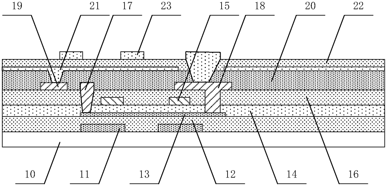
[0073] In this embodiment, an LTPS thin film transistor array substrate with a double gate structure is used to illustrate the technical solution of the embodiment of the present invention. Figure 3-22 It is a schematic diagram of preparing an array substrate according to the first embodiment of the present invention. Among them, the "patterning process" mentioned in this embodiment includes deposition of film layer, coating of photoresist, mask exposure, development, etching, stripping of photoresist, etc., which is an existing mature preparation process. Deposition can use known processes such as sputtering, evaporation, and chemical vapor deposition, coating can use known coating processes, and etching can use known methods, which are not specifically limited here.

[0074] (1) Forming a first electrode and a light-shielding layer pattern on a substrate. Forming the light-shielding layer and the first electrode pattern includes: depositing a first metal film on the substr...

no. 2 example

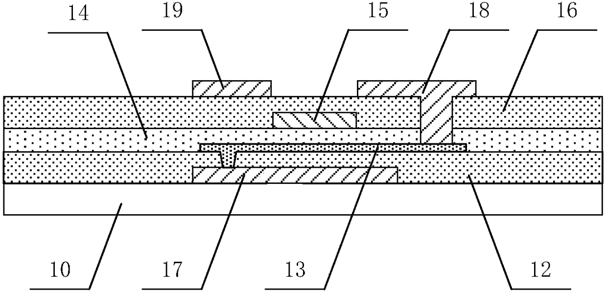
[0101] Figure 23 It is a schematic structural diagram of the second embodiment of the array substrate of the present invention. This embodiment is an extension of the aforementioned first embodiment, and the touch electrodes are disposed above the pixel electrodes. Such as Figure 23 As shown, the array substrate of this embodiment includes: a substrate 10, a light shielding layer 11, a first electrode 17, a buffer layer 12, a U-shaped LTPS active layer 13, a gate insulating layer 14, a gate electrode 15, an interlayer insulating layer 16, The structure of the second electrode 18 and the touch line 19 is the same as that of the aforementioned first embodiment. The fourth via hole connected to the pixel electrode 23, the pixel electrode 23 is arranged on the passivation layer 22, and connected to the second electrode 18 through the fourth via hole, the flat layer 20 covers the pixel electrode 23, and a touch line 19 is opened on it The third via hole connected to the touch ...

no. 3 example

[0104] Although the foregoing embodiments are based on the LTPS thin film transistor array substrate with a double-gate structure, based on the technical concept of the foregoing embodiments, the present invention is also applicable to a single-gate structure. For example, the U-shaped LTPS active layer in the foregoing embodiments can be modified into an L-shaped, the vertical end of the L-shaped active layer is arranged on the source electrode (data line), and forms a cross with the gate electrode (gate line), and The horizontal end is parallel to the gate line without intersecting with the gate line, forming an LTPS thin film transistor array substrate with a single gate structure. In this solution, the source electrode can play a shielding role, so the light shielding layer may not be provided.

[0105] In addition, the embodiments of the present invention are also applicable to array substrates with other structures. The LTPS active layer in the foregoing embodiments can...


PUM


Abstract

The invention provides an array substrate and a preparation method thereof, and a touch control display panel. The array substrate comprises a first electrode and a second electrode for transmitting display signals, and a touch control wire for transmitting touch control signals, the first electrode and the touch control wire are respectively arranged in different layers, and orthographic projections of the first electrode and the touch control wire on the substrate are overlapped. According to the array substrate and the preparation method thereof, and the touch control display panel, the first electrode and the touch control wire are respectively arranged in different layers, and the orthographic projections of the first electrode and the touch control wire on the substrate are overlapped so that the lightproof wiring area is reduced, a light-transmission region is increased, the aperture ratio is increased to the maximum, and the brightness is increased; besides, the first electrodeis adopted as a light-shielding structure so that the area of a light-shielding layer is reduced, the light-transmission region is further increased, adverse display caused by factors including the aligning precision during preparation is effectively avoided, and the yield is increased.

Description

technical field [0001] The present invention relates to the field of display technology, in particular to an array substrate, a preparation method thereof, and a touch display panel. Background technique [0002] With the rapid development of display technology, touch panels (Touch Panel) have gradually spread in people's lives. Touch panels can be classified into add-on mode (Add on Mode), surface-covering type (On Cell), embedded type (InCell) and the like according to the composition structure. Among them, the embedded touch panel is to embed the touch electrodes of the touch module inside the display module, and combine the display and touch into one, which not only greatly reduces the overall thickness of the module, but also makes the product lighter and thinner, and greatly The production cost is reduced. At present, among the in-cell touch panels, the self-capacitive touch panel has gradually become the mainstream touch panel. [0003] The self-capacitive touch pa...

Claims


Application Information

Patent Timeline
Patent Type & Authority Applications(China)
IPC IPC(8): H01L27/12H01L21/77G06F3/041G06F3/044
CPCH01L27/124H01L27/1255H01L27/1259G06F3/0412G06F3/0416G06F3/044G06F2203/04103H01L29/78672H01L29/6675H01L29/78648G06F3/0448G06F3/047
Inventor 武新国王凤国史大为刘弘王子峰李峰马波郭志轩李元博赵晶段岑鸿梁海琴
Owner BOE TECH GRP CO LTD
Why Eureka
Try Eureka