Preparation method for etching liquid for thin film transistor

A technology for thin film transistors and etching solution, which is applied in the field of preparation of etching solution for thin film transistors, can solve the problems of poor metal trace etching effect, rough surface of chromium metal film, photoresist peeling, etc., and achieves high etching speed. Controllability, improved etching effect, reduced surface tension effect

Inactive Publication Date: 2018-06-12
佛山杰致信息科技有限公司
View PDF2 Cites 3 Cited by
  • Summary
  • Abstract
  • Description
  • Claims
  • Application Information

AI Technical Summary

Problems solved by technology

The main disadvantages of this type of etching solution for etching chromium metal films are: the etching speed is slow, causing the photoresist to be soaked in the etching solution for a long time, which will cause part of the photoresist to fall off and cause some metal wiring to be damaged. The etching effect is not good; there are also etching marks on the interface between the anti-corrosion coating and the chromium metal film that do not need to be etched due to the infiltration of the etching solution, resulting in rough surface of the chromium metal film that does not need to be etched

Method used


Image

  • Preparation method for etching liquid for thin film transistor

Examples


Embodiment 1

[0019] The preparation method of above-mentioned etchant for thin film transistor comprises the following steps:

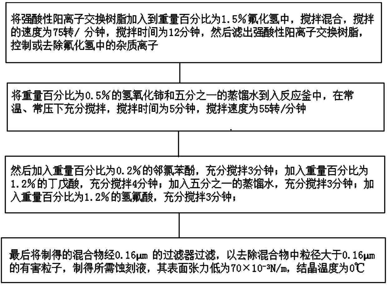
[0020] The first step: add the strong acidic cation exchange resin to 1.5% hydrogen fluoride by weight, stir and mix, the stirring speed is 75 rpm, and the stirring time is 12 minutes, then filter out the strong acidic cation exchange resin, control or remove Impurity ions in hydrogen fluoride;

[0021] The second step: put 0.5% cerium hydroxide and 1 / 5 distilled water into the reaction kettle, fully stir at normal temperature and pressure, the stirring time is 5 minutes, and the stirring speed is 55 rpm;

[0022] The third step: then add 0.2% o-chlorophenol by weight, and fully stir for 3 minutes; add 1.2% by weight of valeric acid, fully stir for 4 minutes; add 1 / 5 of distilled water, and fully stir for 3 minutes; Add 1.2% by weight of hydrofluoric acid, fully stir for 3 minutes; add 1.5% by weight of hydrogen fluoride, fully stir for 4 minutes; add 2.5% by wei...

Embodiment 2

[0029] The preparation method of above-mentioned etchant for thin film transistor comprises the following steps:

[0030] The first step: add the strong acidic cation exchange resin to 1.9% hydrogen fluoride by weight, stir and mix, the stirring speed is 82 rpm, and the stirring time is 17 minutes, then filter out the strong acidic cation exchange resin, control or remove Impurity ions in hydrogen fluoride;

[0031] Step 2: put 1.5% cerium hydroxide and 1 / 5 distilled water into the reaction kettle, stir fully at normal temperature and pressure, the stirring time is 8 minutes, and the stirring speed is 60 rpm;

[0032] The third step: then add 1.2% o-chlorophenol by weight and fully stir for 4 minutes; add 1.9% by weight valeric acid and fully stir for 5 minutes; add 1 / 5 of distilled water and fully stir for 4 minutes; Add 2.0% by weight of hydrofluoric acid, fully stir for 3.5 minutes; add 1.5% by weight of hydrogen fluoride, fully stir for 4 minutes; add 2.5% by weight of no...

Embodiment 3

[0039] The preparation method of above-mentioned etchant for thin film transistor comprises the following steps:

[0040] The first step: add the strong acidic cation exchange resin to 2.3% hydrogen fluoride by weight, stir and mix, the stirring speed is 90 rpm, and the stirring time is 20 minutes, then filter out the strong acidic cation exchange resin, control or remove Impurity ions in hydrogen fluoride;

[0041]The second step: put 2.3% cerium hydroxide and 1 / 5 distilled water into the reaction kettle, fully stir at normal temperature and pressure, the stirring time is 10 minutes, and the stirring speed is 65 rpm;

[0042] The third step: then add 1.8% o-chlorophenol by weight and fully stir for 5 minutes; add 2.6% valeric acid by weight and fully stir for 6 minutes; add 1 / 5 of distilled water and fully stir for 5 minutes; Add 2.6% by weight of hydrofluoric acid, fully stir for 4 minutes; add 2.3% by weight of hydrogen fluoride, fully stir for 6 minutes; add 3.3% by weigh...


PUM

PropertyMeasurementUnit
particle diameteraaaaaaaaaa
surface tensionaaaaaaaaaa
crystallization temperatureaaaaaaaaaa

Abstract

The invention discloses a preparation method for etching liquid for a thin film transistor. The etching liquid comprises the following compositions in percentage by weight: 0.5%-2.3% of cerium hydroxide, 0.2%-1.8% of o-chlorophenol, 1.2%-2.6% of isobutylglutaric acid, 1.2%-2.6% of hydrofluoric acid, 1.5%-2.3% of hydrogen fluoride, 2.5%-3.3% of a nonionic surfactant, 1.5%-2.6% of a de-foaming agentand the balance of distilled water. Cerium hydroxide, o-chlorophenol, isobutylglutaric acid, hydrofluoric acid and hydrogen fluoride are added on the basis of the original process, so that etching can be performed when penetration of an anti-corrosion coating does not occur, and etching speed of a chromium metal film is remarkably increased, and therefore, the preparation method has controllableetching speed, effectively inhibits degradation of an anti-corrosion protective layer, obtains a chromium metal film assembly line with a flat and smooth surface, and has an important application value.

Description

technical field [0001] The invention relates to a preparation method of an etching solution for a thin film transistor. Background technique [0002] Thin-film transistor (Thin-film transistor) is widely used in notebook computers, LCD TVs, etc. More and more users of all ages. Thin film transistors are key devices in thin film transistors, and their performance is decisive for the performance of the final thin film transistor product. The manufacturing process is to manufacture different thin films on the glass substrate according to the optical and electrical characteristics of the device, and process the different thin films according to the design requirements to form a regularly arranged specific electronic device - thin film transistor array. The main process of thin film transistor array manufacturing includes basic steps such as substrate cleaning, film formation, photolithography, inspection and repair. The core process is photolithography. In the manufacturing ...

Claims


Application Information

Patent Timeline
Patent Type & Authority Applications(China)
IPC IPC(8): C23F1/26
CPCC23F1/26
Inventor 刘威
Owner 佛山杰致信息科技有限公司
Why Eureka
Try Eureka