Through-silicon-via technique based three-dimensional band-pass filter

A band-pass filter and through-silicon via technology, which is applied in the field of three-dimensional band-pass filters, can solve the problems of inability to apply coupling capacitor band-pass filter design, high cost of process preparation, extra cost of silicon wafers, etc., so as to improve high-frequency Stop-band suppression characteristics, reducing the occupied area, and realizing the effect of effective utilization

Active Publication Date: 2018-06-22
NINGBO UNIV
View PDF8 Cites 13 Cited by
  • Summary
  • Abstract
  • Description
  • Claims
  • Application Information

AI Technical Summary

Problems solved by technology

Although this design method can reduce the size of capacitors and low-pass filters, there are still some shortcomings: First, the coaxial silicon vias used in this patent belong to a non-standard silicon via structure, and its structure includes the first dielectric layer, The outer metal layer, the second dielectric layer and the metal core layer are electrically isolated by filling the first dielectric layer between the silicon substrate and the outer metal layer, and filling the second dielectric layer between the outer metal layer and the metal core layer. The outer metal layer must Grounding, when used as a capacitor design and application, the metal core layer is used as the upper plate electrode of the capacitor, and the outer metal layer is used as the lower plate electrode of the capacitor. This structure determines that the coaxial TSV capacitor is only suitable for grounding capacitor design and cannot be used for coupling Capacitors and band-pass filter designs including coup

Method used


Image

  • Through-silicon-via technique based three-dimensional band-pass filter
  • Through-silicon-via technique based three-dimensional band-pass filter
  • Through-silicon-via technique based three-dimensional band-pass filter

Examples


Embodiment 1

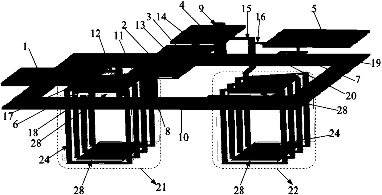
[0022] The three-dimensional bandpass filter based on TSV technology of embodiment 1, such as figure 1 As shown, it includes a parallel plate capacitor unit, a planar spiral inductor unit, a rewiring layer, a three-dimensional solenoid inductor unit, and a soft ferrite material unit.

[0023] The parallel plate capacitor unit includes a first capacitor 1, a second capacitor 2, a third capacitor 3, a fourth capacitor 4, and a fifth capacitor 5. The planar spiral inductor unit includes a first planar spiral inductor 6 and a second planar spiral inductor 7 (such as Figure 4 (Shown), the rewiring layer includes an input terminal 8, an output terminal 9, a grounded metal line 10, and a horizontally arranged first metal interconnection layer 11, a second metal interconnection layer 12, a third metal interconnection layer 13, and a fourth metal interconnection layer. Metal interconnection layer 14, fifth metal interconnection layer 15, sixth metal interconnection layer 16, seventh metal...


PUM


Abstract

The invention discloses a through-silicon-via technique based three-dimensional band-pass filter, which comprises a parallel-plate capacitor unit, a planar spiral inductor unit, a rewiring layer, a three-dimensional solenoid inductor unit and a soft magnetic ferrite unit. The three-dimensional band-pass filter realizes three-dimensional solenoid inductors through on-chip redundancy through siliconvia, and the occupied area of the three-dimensional solenoid inductors is remarkably reduced through the through silicon via in vertical arrangement and metal interconnection layers in horizontal arrangement; by adding of high-permeability soft magnetic ferrite into the three-dimensional solenoid inductors, permeability and inductance density of the three-dimensional solenoid inductors are further improved. The three-dimensional band-pass filter is excellent in high-frequency stop-band suppression characteristic and frequency selectivity and is up to 31.6% in relative bandwidth ratio and up to 100nH/mm<2> in inductor inductance density. The three-dimensional band-pass filter has advantages of small occupied area, low loss and compact size and is applicable to high-performance radio-frequency circuit design and application.

Description

Technical field [0001] The invention relates to the technical field of filter design in microwave circuits, in particular to a three-dimensional band-pass filter based on silicon through hole technology. Background technique [0002] Modern wireless communication equipment and communication systems have the advantages of miniaturization, high speed and multi-function, and usually support different communication protocols. In order to develop such communication equipment and communication systems, the industry has proposed a series of advanced packaging technologies such as system-in-package, on-chip packaging and three-dimensional integration. However, due to the large size of inductors and capacitors, these packaging technologies still cannot integrate RF passive units such as filters, couplers, and antennas into the system. For this reason, CN106158835A proposes a low-pass filter based on through-silicon via technology, using vertical coaxial through-silicon via capacitors ins...

Claims


Application Information

Patent Timeline
IPC IPC(8): H01L23/64H01L25/04H01P1/20
CPCH01L23/64H01L23/642H01L23/645H01L25/04H01P1/20
Inventor 钱利波桑吉飞励达何锡涛
Owner NINGBO UNIV
Why Eureka
Try Eureka