Fabrication process of high-brightness LED

A preparation process and high-brightness technology, applied in the field of lighting, can solve the problems of commercial production, high preparation cost, complicated process, etc., and achieve reduced production cost and process complexity, easy controllable wavelength, and indium component content stable effect

Active Publication Date: 2018-06-22
廊坊熙泰科技有限公司
View PDF7 Cites 7 Cited by
  • Summary
  • Abstract
  • Description
  • Claims
  • Application Information

AI Technical Summary

Problems solved by technology

However, at the present stage, the preparation cost of graphene thin film layer is high and the process is complicated, and commercial production cannot be realized. At the same time, the installation of graphene thin film layer is easy to cause other problems such as carbon contamination. It is necessary to seek other alternative means to improve LED luminous efficiency.

Method used


Image

  • Fabrication process of high-brightness LED
  • Fabrication process of high-brightness LED
  • Fabrication process of high-brightness LED

Examples


Embodiment 1

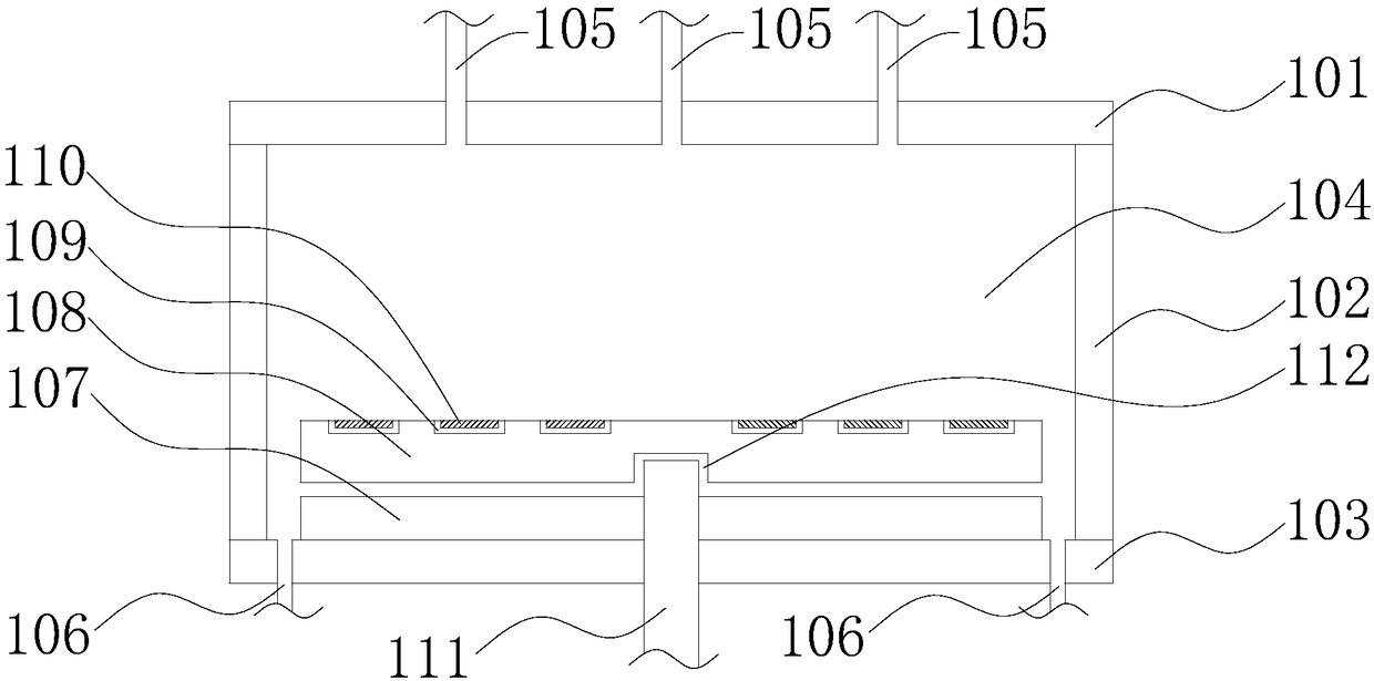
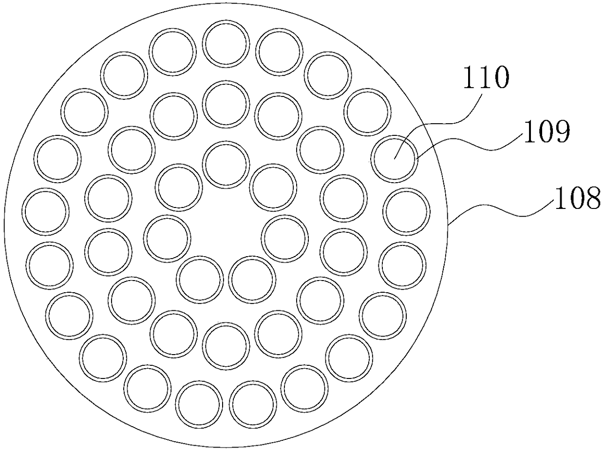
[0029] Please refer to figure 1 , figure 2 , when manufacturing LEDs by MOCVD (Metal Organic Chemical Vapor Deposition, Metal Organic Chemical Vapor Deposition) equipment, the substrate 110 is first placed in the grooves 109 evenly distributed on the carrier plate 108, and the depth of the grooves 109 is slightly higher than that of the substrate. The thickness of the bottom 110, the size of the substrate 110 can be two inches, four inches or six inches, and the slide disc 108 is made of high temperature resistant material, such as graphite. Then transfer the slide tray 108 with the substrate 110 into the reaction chamber 104. The reaction chamber 104 is a closed structure formed by the upper cover 101, the side wall 102 and the base 103. Trachea 105, reaction gas, carrier gas (NH3, N2, H2, etc.) and MO source (trimethylgallium, triethylgallium, trimethylaluminum, trimethylindium, dimagnesium, etc.) The reaction in the reaction chamber 104 is then deposited on the substrate...


PUM


Abstract

The invention provides a fabrication process of a high-brightness LED. The fabrication process comprises the step of sequentially depositing a buffer layer, an N-type GaN layer, a light-emitting layerand a P-type GaN layer on a substrate by a metal organic chemical vapor deposition process, wherein the substrate is placed on a rotating slide disc, the light-emitting layer comprises a quantum welllayer and a quantum barrier layer which are periodically laminated, at least one of the quantum well layer and the quantum barrier layer which are periodically laminated is a high-speed quantum welllayer and a low-speed quantum well layer, and the rotational speed of the slide disc during forming the high-speed quantum well layer is larger than the rotational speed of the slide disc during forming the low-speed quantum well layer. Indium is doped into gallium nitride by increasing the rotational speed, the indium doping quantity is prevented from being increased by reducing a growth temperature, the quantum well layer is deposited under a higher temperature, and the obtained quantum well layer is better in crystal quality; and meanwhile, the fabrication process is low in cost and is easyto implement.

Description

technical field [0001] The invention relates to the technical field of lighting, in particular to a high-brightness LED preparation process. Background technique [0002] LED (LightingEmittingDiode) lighting is light-emitting diode lighting, which is a semiconductor solid-state light-emitting device. It uses a solid semiconductor chip as a light-emitting material. In the semiconductor, the excess energy is released through the recombination of carriers to cause photon emission, and directly emits red, yellow, blue, and green light. On this basis, using the principle of three primary colors, Adding fluorescent powder can emit light of any color. The lighting fixtures manufactured using LEDs as light sources are LED lamps. [0003] The LED manufacturing process is divided into epitaxy, chip front-end, chip back-end, packaging and other links. Epitaxy deposits a buffer layer, an N-type GaN layer, a light-emitting layer, and a P-type GaN layer on a sapphire substrate through a...

Claims


Application Information

Patent Timeline
Patent Type & Authority Applications(China)
IPC IPC(8): H01L33/00H01L33/06H01L33/32
CPCH01L33/007H01L33/06H01L33/325
Inventor 李丹丹
Owner 廊坊熙泰科技有限公司
Why Eureka
Try Eureka