Semiconductor device and method of forming the same

A technology of semiconductors and devices, which is applied in the field of semiconductor devices and their formation, can solve the problems that the electrical properties of semiconductor devices need to be improved, and achieve the effects of reducing defect content, improving quality, and improving interface performance

Active Publication Date: 2020-10-09
SEMICON MFG INT (SHANGHAI) CORP +1
View PDF3 Cites 0 Cited by
  • Summary
  • Abstract
  • Description
  • Claims
  • Application Information

AI Technical Summary

Problems solved by technology

However, the electrical performance of semiconductor devices formed by existing technologies needs to be improved

Method used


Image

  • Semiconductor device and method of forming the same
  • Semiconductor device and method of forming the same
  • Semiconductor device and method of forming the same

Examples


Embodiment Construction

[0030] It can be seen from the background art that the electrical performance of semiconductor devices formed in the prior art needs to be improved.

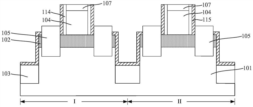
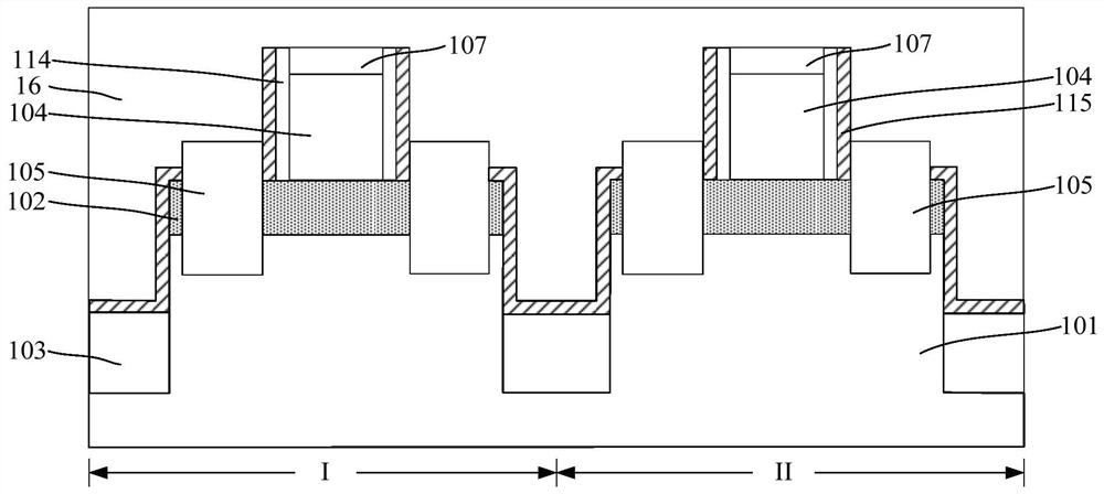
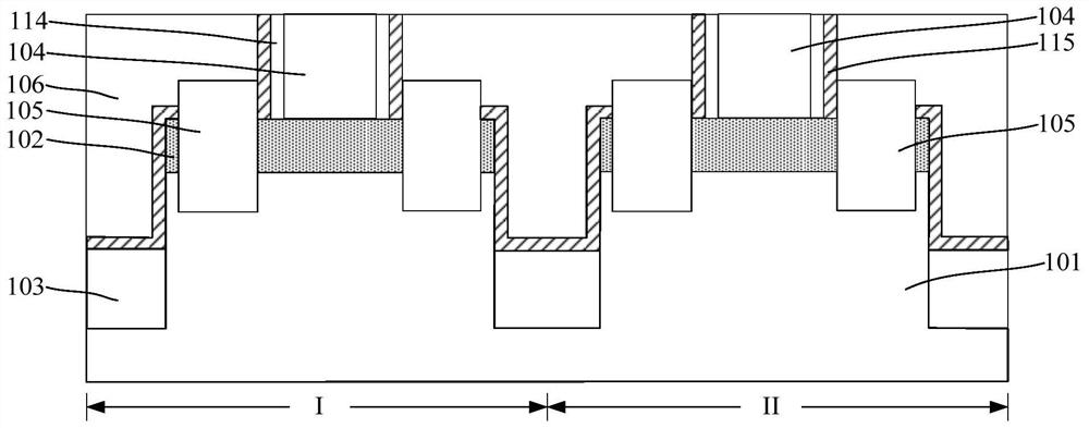
[0031] After analysis, when silicon germanium is used as the material of the channel region, in order to improve the interface performance between the channel region and the high-k gate dielectric layer and improve the quality of the formed high-k gate dielectric layer, before forming the high-k gate dielectric layer The surface of the silicon germanium material is oxidized, and an oxygen-containing silicon germanium layer is formed between the silicon germanium channel region and the high-k gate dielectric layer as an interface layer. Generally, the oxygen-germanium-containing silicon layer is formed by a thermal oxidation process, and the formed oxygen-germanium-containing silicon layer has many defects, so that the electrical performance of the formed semiconductor device is still poor.

[0032] In order to solve the above pr...


PUM

PropertyMeasurementUnit
thicknessaaaaaaaaaa
thicknessaaaaaaaaaa

Abstract

The present invention provides a semiconductor device and a formation method thereof. The formation method comprises the steps of: providing a base, wherein the base comprises a substrate and a germanium-silicon layer located on the substrate; performing oxidation treatment of the germanium-silicon layer, and forming an oxygen-containing germanium-silicon layer on the germanium-silicon layer; performing reduction treatment of the surface of the germanium-silicon layer, and reducing the germanium content in the oxygen-containing germanium-silicon layer; after the reduction treatment, forming ahigh k-gate medium layer on the oxygen-containing germanium-silicon layer; and forming a metal gate on the high k-gate medium layer. The semiconductor device and the formation method thereof improve the interface performances between a germanium-silicon channel region and the high k-gate medium layer and improve the quality of the formed high k-gate medium layer so as to improve the electrical properties of the formed semiconductor device.

Description

technical field [0001] The invention relates to the technical field of semiconductor manufacturing, in particular to a semiconductor device and a forming method thereof. Background technique [0002] The main semiconductor device of an integrated circuit, especially a very large scale integrated circuit, is a metal-oxide-semiconductor field effect transistor (MOS transistor). With the continuous development of integrated circuit manufacturing technology, the technology nodes of semiconductor devices are continuously reduced, and the geometric dimensions of semiconductor structures are continuously reduced following Moore's law. When the size of the semiconductor structure is reduced to a certain extent, various secondary effects caused by the physical limit of the semiconductor structure appear one after another, and it becomes more and more difficult to scale down the feature size of the semiconductor structure. Among them, in the field of semiconductor manufacturing, the ...

Claims


Application Information

Patent Timeline
Patent Type & Authority Patents(China)
IPC IPC(8): H01L21/02H01L21/336H01L29/78H01L29/423
CPCH01L21/0245H01L21/02664H01L29/4232H01L29/66477H01L29/78
Inventor 李勇
Owner SEMICON MFG INT (SHANGHAI) CORP
Why Eureka
Try Eureka