Visible-infrared broadband absorber and preparation method thereof

An absorber and broadband technology, applied in the fields of photothermal conversion and optical devices, can solve the problems of cumbersome preparation, difficulty in large-area production, complex structure, etc., and achieve the effects of simple process, shortened production cycle and high absorption efficiency.

Inactive Publication Date: 2018-07-20
XUZHOU NORMAL UNIVERSITY
View PDF4 Cites 3 Cited by
  • Summary
  • Abstract
  • Description
  • Claims
  • Application Information

AI Technical Summary

Problems solved by technology

However, the structure of this type of absorber is complex, the preparation is cumbersome, and it is difficult to produce on a large scale in practical applications.
Therefore, it is still a major challenge in this field to design a structure that is simple, easy to fabricate, and low-cost with high-efficiency broad-spectrum absorbing structures.

Method used


Image

  • Visible-infrared broadband absorber and preparation method thereof
  • Visible-infrared broadband absorber and preparation method thereof
  • Visible-infrared broadband absorber and preparation method thereof

Examples


Embodiment 1

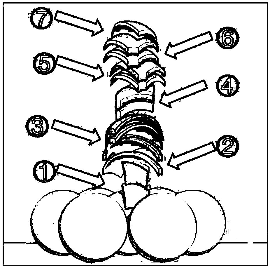
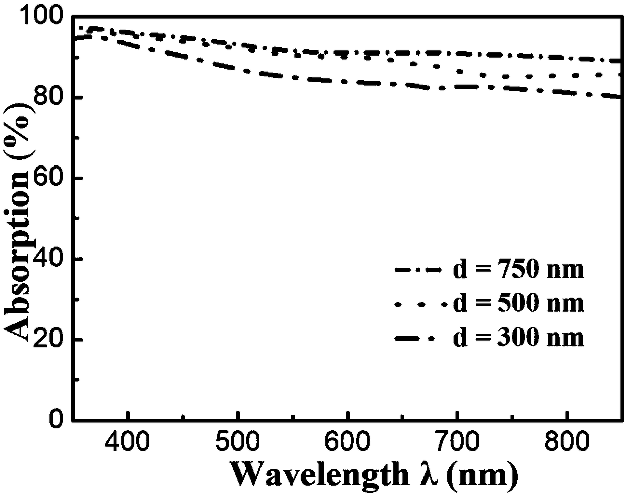
[0023] A monolayer film of polystyrene spheres was prepared on a glass slide as a substrate. The spheres we used were aqueous solution of polystyrene spheres produced by HugeBiotechnology Company, and the diameter of the spheres was d=300nm. The metal absorption layer / non-metal dielectric layer unit is deposited on the substrate by thermal evaporation, and the substrate is rotated so that the optimal angle between the normal and the deposition direction is 75°. Each metal absorption layer / non-metal dielectric layer unit sample The azimuth rotation angle of the stage increases by 65° each time, and there are 7 metal absorption layer / non-metal dielectric layer units in total, and the thickness of each layer of the alternate metal absorption layer / non-metal dielectric layer is optimized to 30nm. attached figure 1 It is a schematic structural diagram of an ultra-broadband absorber in the visible to near-infrared band of the present invention. ①-⑦ in the figure represent 7 metal a...

Embodiment 2

[0025] A monolayer film of polystyrene spheres was prepared on a glass slide as a substrate. The spheres we used were aqueous solution of polystyrene spheres produced by HugeBiotechnology Company, and the diameter of the spheres was d=500nm. The metal absorption layer / non-metal dielectric layer unit is deposited on the substrate by thermal evaporation, and the substrate is rotated so that the optimal angle between the normal and the deposition direction is 75°. Each metal absorption layer / non-metal dielectric layer unit sample The azimuth rotation angle of the stage increases by 65° each time, and there are 7 metal absorption layer / non-metal dielectric layer units in total, and the thickness of each layer of the alternate metal absorption layer / non-metal dielectric layer is optimized to 30nm. attached figure 1 It is a schematic structural diagram of an ultra-broadband absorber in the visible to near-infrared band of the present invention. ①-⑦ in the figure represent 7 metal a...

Embodiment 3

[0027] A monolayer film of polystyrene spheres was prepared on a glass slide as a substrate. The spheres we used were aqueous solution of polystyrene spheres produced by HugeBiotechnology Company, and the diameter of the spheres was d=750nm. The metal absorption layer / non-metal dielectric layer unit is deposited on the substrate by thermal evaporation, and the substrate is rotated so that the optimal angle between the normal and the deposition direction is 75°. Each metal absorption layer / non-metal dielectric layer unit sample The azimuth rotation angle of the stage increases by 65° each time, and there are 7 metal absorption layer / non-metal dielectric layer units in total, and the thickness of each layer of the alternate metal absorption layer / non-metal dielectric layer is optimized to 30nm. attached figure 1 It is a schematic structural diagram of an ultra-broadband absorber in the visible to near-infrared band of the present invention. figure 1 Middle ①-⑦ represent 7 metal...


PUM

PropertyMeasurementUnit
diameteraaaaaaaaaa
thicknessaaaaaaaaaa

Abstract

The invention discloses a visible-infrared broadband absorber and a preparation method thereof. The absorber comprises a substrate; a polystyrene pellet single-layer film layer and an alternating filmlayer formed by mutual alternating of metal absorption layers and non-metal dielectric layers are arranged successively on the substrate from top to bottom; a metal dielectric layer approaches the bottom polystyrene pellet single-layer film layer; each metal absorption layer is formed by one or more metal absorbing layer units; and each non-metal dielectric layer is formed by one or more metal absorbing layer units. The absorber has advantages of high absorption efficiency, wide working band, simple process, low cost and large area preparation and the like. Compared with the traditional broadband absorber, the absorber having a compact multi-layer film structure has the following beneficial effects: the production cost is lowered obviously; the production cycle is shortened substantially;and large-scale batched production can be realized.

Description

technical field [0001] The invention relates to the technical fields of light-to-heat conversion and optical devices, in particular to a broadband absorber in visible to infrared bands and a preparation method. Background technique [0002] With the rapid development of modern science and technology, broadband perfect absorbers have always been a hot topic in the field of science and technology. Important application requirements have attracted widespread attention. [0003] In recent years, various absorbing structures have been designed, such as planar metal / dielectric structures, reflective metal grating structures, metamaterial structures, and surface plasmon-based structures. There are many schemes to achieve total absorption based on plasmonic metamaterial systems, and the metal particle-dielectric layer-metal layer metamaterial system is one of the typical structures to achieve superabsorption. Compared with traditional methods, this system has sub-wavelength charac...

Claims


Application Information

Patent Timeline
Patent Type & Authority Applications(China)
IPC IPC(8): G02B5/00
CPCG02B5/003
Inventor 韩彩芹王洪峰闫长春赵奕平
Owner XUZHOU NORMAL UNIVERSITY
Why Eureka
Try Eureka