A method for preparing strained silicon by high-energy X-rays

An X-ray and strained silicon technology, which is applied in the field of high-energy X-ray preparation of strained silicon, can solve the problems of difficult removal of impurities and particle contamination, brittle and easy cracking of the silicon nitride cap layer, and small strain, achieving short exposure time, Fast straining process and high production efficiency

Active Publication Date: 2019-04-09
XI AN JIAOTONG UNIV
View PDF3 Cites 0 Cited by
  • Summary
  • Abstract
  • Description
  • Claims
  • Application Information

AI Technical Summary

Problems solved by technology

The advantage of the stress capping layer technology is that the mobility of silicon in both n and p channels is improved. The disadvantage is that different methods of capping layer deposition process may introduce high temperature, or it is difficult to remove impurities and particle contamination, or the cost is too high. And the silicon nitride cap layer is brittle and easy to break, causing stress release and reducing the strain (D A Antoniadis, I Aberg, C Ni Chleirigh, et al. Continuous MOSFET performance increase with device scaling: the role of strain and channel material innovation[J]. IBM Journal of Research and Development, 2006)

Method used


Image

  • A method for preparing strained silicon by high-energy X-rays
  • A method for preparing strained silicon by high-energy X-rays
  • A method for preparing strained silicon by high-energy X-rays

Examples


Embodiment Construction

[0019] In the following, the present invention will be further described by using two embodiments in combination with the accompanying drawings and specific implementation methods.

[0020] The first embodiment specifically includes the following steps:

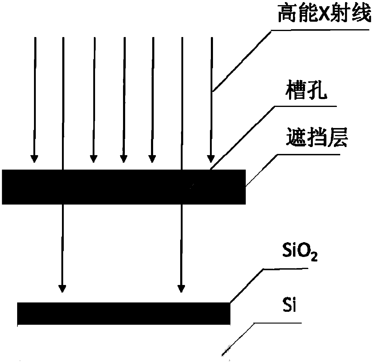
[0021] Step (1) synthesizes a Si / SiO2 double-layer composite structure system, which is synthesized by a known dry oxygen oxidation method, such as figure 1 As shown, its structure is a silicon film covered with a silicon dioxide layer on the upper surface. The thickness of the silicon film is 2 μm, the thickness of the silicon dioxide layer is 0.45 μm, and the size is 4.7mm×4.7mm. The Si / SiO2 double-layer composite structure system , the details of the synthesis process are as follows:

[0022] Take an 8-inch N-type low-resistance double-sided polished silicon wafer, perform standard cleaning on the silicon wafer, remove the surface oxide layer with HF (1:100), and dry it after blowing with nitrogen to complete the wafer p...


PUM

PropertyMeasurementUnit
thicknessaaaaaaaaaa
thicknessaaaaaaaaaa
thicknessaaaaaaaaaa

Abstract

The invention discloses a method for preparing strained silicon by high energy X ray, and relates to the manufacturing field of an integrated circuit. The method comprises the following steps of (1) synthesizing a Si / SiO<2> dual-layer composite structural system, wherein the upper surface of the structure is covered with a silicon thin film of a silicon dioxide layer; (2) if partial strain needs to occur, placing a shielding layer above the Si / SiO<2> dual-layer composite structural system, and forming a groove hole with the corresponding dimension and shape in the shielding layer above the required strain region of the silicon thin film; and if global strain needs to occur, not placing the shielding layer; and (3) performing illumination on the Si / SiO<2> dual-layer composite structural system by high energy X ray through the shielding layer to prepare strained silicon. By virtue of the initial application of the method of the high energy X ray, by combination of the method of region-selecting shielding, and by virtue of the characteristic that the X ray beam spot area is larger than the dimension of a silicon wafer, quick preparation of strained silicon is realized; and the methodhas the advantages of low working temperature, controllable strain region, no introduction of impurity, simple process, large scope of variables, high production efficiency, no silicon damage and thelike, and is expected to be widely applied to the fields of a semiconductor integrated circuit, a micro-nano electronic device and the like.

Description

technical field [0001] The invention relates to the field of integrated circuit manufacturing, in particular to a method for preparing strained silicon with high-energy X-rays. Background technique [0002] Silicon is an extremely important raw material in the semiconductor manufacturing industry today. With the continuous development and improvement of chip manufacturing technology, the emergence of strained silicon technology has become an effective means to further increase the speed of chip operation. When the silicon lattice is strained by stress, the effective mass of transport carriers can be reduced, and the mobility and saturation velocity can both be increased. Therefore, under the same device size, if the strained silicon technology is used as the carrier transport channel, the goal of increasing the device speed and driving current can be achieved because of the increase in the carrier mobility of electrons and holes. [0003] At present, there are mainly two ty...

Claims


Application Information

Patent Timeline
Patent Type & Authority Patents(China)
IPC IPC(8): H01L21/268
CPCH01L21/2683
Inventor 陈凯潘志豪朱文欣
Owner XI AN JIAOTONG UNIV
Why Eureka
Try Eureka