A kind of preparation method of light-emitting diode epitaxial wafer

A technology of light-emitting diodes and epitaxial wafers, which is applied in semiconductor devices, electrical components, circuits, etc., can solve the problems of reducing the luminous efficiency of light-emitting diodes, affecting the recombination efficiency of electrons and holes, and poor growth quality of multiple quantum well layers. Polarization effect, luminous efficiency improvement, stress relief effect

Active Publication Date: 2020-01-10
HC SEMITEK SUZHOU
View PDF3 Cites 0 Cited by
  • Summary
  • Abstract
  • Description
  • Claims
  • Application Information

AI Technical Summary

Problems solved by technology

[0005] The buffer layer is an aluminum nitride layer or a gallium nitride layer. Since the metal polar surface (aluminum polar surface or gallium polar surface) is smoother than the non-metal polar surface (nitrogen polar surface), the stability Better, so the surface of the buffer layer setting undoped GaN layer is usually a metal polar surface, so that the stress and defects generated by the lattice mismatch between the substrate and GaN can easily extend to the MQW layer, The growth quality of the multi-quantum well layer is poor, resulting in a polarization effect, and the overlap of the electronic wave function of the multi-quantum well layer is weakened, which affects the recombination efficiency of electrons and holes, and reduces the luminous efficiency of the light-emitting diode.

Method used


Image

  • A kind of preparation method of light-emitting diode epitaxial wafer

Examples


Embodiment 1

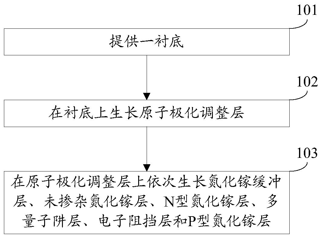
[0035] The embodiment of the present invention provides a method for preparing a light-emitting diode epitaxial wafer, figure 1 For the flow chart of the preparation method provided by the embodiments of the present invention, see figure 1 , the preparation method comprises:

[0036] Step 101: Provide a substrate.

[0037] Optionally, this step 101 may include:

[0038] An aluminum nitride film is formed on a sapphire substrate by using a physical vapor deposition (English: Physical Vapor Deposition, PVD for short) technique.

[0039] The aluminum nitride thin film is preformed on the sapphire substrate by PVD technology, and the subsequent atomic polarization adjustment layer is grown on the aluminum nitride thin film, which is beneficial to the growth of the atomic polarization adjustment layer and improves the growth quality of the epitaxial wafer.

[0040] Step 102: growing an atomic polarization adjustment layer on the substrate.

[0041] In this embodiment, the atomi...

Embodiment 2

[0069] An embodiment of the present invention provides a method for preparing a light-emitting diode epitaxial wafer, and the preparation method provided in this embodiment is a specific realization of the preparation method provided in Embodiment 1. Specifically, the preparation method includes:

[0070] Step 200: Treat the surface of the substrate with ammonia gas.

[0071] Step 201: controlling the temperature to 1200° C., the pressure to 200 Torr, and the V / III ratio to 1200, using ammonia gas and trimethylaluminum to grow an atomic polarization adjustment layer with a thickness of 100 nm.

[0072] Step 202 : controlling the temperature to 500° C. and the pressure to 500 Torr, growing a gallium nitride buffer layer with a thickness of 100 nm on the atomic polarization adjustment layer.

[0073] Step 203: Control the temperature to 1050° C. and the pressure to 300 Torr, and grow an undoped GaN layer with a thickness of 1 μm on the GaN buffer layer.

[0074] Step 204: Cont...

Embodiment 3

[0083] The embodiment of the present invention provides a method for preparing a light-emitting diode epitaxial wafer, and the preparation method provided in this embodiment is another specific realization of the preparation method provided in the first embodiment. The preparation method provided in this example is basically the same as that provided in Example 2, except that, in this example, the growth temperature of the atomic polarization adjustment layer is 1100° C., and the V / III ratio is 400.

[0084] Experiments have found that compared with Example 2, the beneficial effect is increased by about 5%.


PUM

PropertyMeasurementUnit
thicknessaaaaaaaaaa
thicknessaaaaaaaaaa
thicknessaaaaaaaaaa

Abstract

The invention discloses a preparation method of a light emitting diode epitaxial wafer, and belongs to the technical field of a semiconductor. The preparation method comprises the steps of providing asubstrate; enabling an atomic polarized adjustment layer to be grown on the substrate, wherein the atomic polarized adjustment layer is a compound formed by metal elements and a nitrogen element, themetal elements comprise at least one of aluminum and gallium, and the surface, opposite to the surface arranged on the substrate, of the atomic polarized adjustment layer is a nitrogen polarized surface; and performing growth of a gallium nitride buffer layer, a non-doped gallium nitride layer, an N type gallium nitride layer, a multi-quantum-well layer, an electron barrier layer and a P type gallium nitrogen layer on the atomic polarized adjustment layer in sequence. By virtue of the atomic polarized adjustment layer, the stress generated by lattice mismatch between the substrate and galliumnitride is released, so that spreading of dislocation and defects generated by lattice mismatch between the substrate and gallium nitride to the multi-quantum-well layer can be suppressed, thereby improving the growth quality of the multi-quantum-well layer, avoiding a polarization effect, and improving the luminous efficiency of the light emitting diode.

Description

technical field [0001] The invention relates to the technical field of semiconductors, in particular to a method for preparing a light-emitting diode epitaxial wafer. Background technique [0002] Light Emitting Diode (English: Light Emitting Diode, referred to as: LED) is a semiconductor light emitting device made by using the principle of semiconductor PN junction electroluminescence. The epitaxial wafer is the primary product in the process of manufacturing light-emitting diodes. [0003] The existing epitaxial wafer includes a sapphire substrate and a buffer layer, an undoped gallium nitride layer, an n-type gallium nitride layer, a multi-quantum well layer, an electron blocking layer and a p-type gallium nitride layer stacked on the sapphire substrate in sequence. Floor. Wherein, the multi-quantum well layer includes multiple quantum wells and multiple quantum barriers, the multiple quantum wells and multiple quantum barriers are alternately stacked, the quantum wells...

Claims


Application Information

Patent Timeline
Patent Type & Authority Patents(China)
IPC IPC(8): H01L33/00H01L33/12H01L33/22
CPCH01L33/005H01L33/12H01L33/22
Inventor 郭炳磊王群李鹏
Owner HC SEMITEK SUZHOU
Why Eureka
Try Eureka