Preparation method of core-shell GaN nanowire array

A nanowire array and core-shell technology, which is applied in the field of electricity, can solve problems such as the difficulty in preparing high-quality, orderly arranged core-shell GaN nanowire arrays, and achieve significant technological progress, simple process, and simple and easy methods

Inactive Publication Date: 2018-08-14
UNIV OF SHANGHAI FOR SCI & TECH
View PDF8 Cites 5 Cited by
  • Summary
  • Abstract
  • Description
  • Claims
  • Application Information

AI Technical Summary

Problems solved by technology

However, these methods are difficult to prepare high-quality, ordere

Method used


Image

  • Preparation method of core-shell GaN nanowire array
  • Preparation method of core-shell GaN nanowire array
  • Preparation method of core-shell GaN nanowire array

Examples


Embodiment 1

[0029] Example 1 Fabrication of a core-shell GaN nanowire array with a quantum well structure with a nanowire diameter less than 200 nm and a height of 4 μm

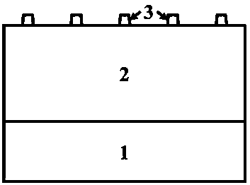
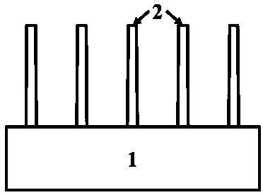
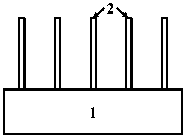
[0030] Figure 1~4 It is a flow chart for preparing a core-shell GaN nanowire array, and a method for preparing a core-shell GaN nanowire array of the present invention includes the following steps:

[0031] 1) if figure 1 As shown, the metal organic vapor phase chemical deposition (MOCVD) method is used to epitaxially buffer layer and n-GaN 2 on the Si substrate 1 in sequence, with a total thickness of about 6 μm;

[0032] 2) 1 μm thick SiO was grown on the epitaxial layer by CVD method 2 Mask layer 3, preparing a circular mask pattern with a diameter of 5 μm by photolithography and ICP etching process;

[0033] 3) Use buffered oxide etchant BOE to etch SiO 2 The mask layer 3 is etched for 5min and 50s at a temperature of 22°C to prepare a mask with a size of about 500 nm;

[0034] 4) The GaN-based epitaxial layer ...


PUM

PropertyMeasurementUnit
Sizeaaaaaaaaaa

Abstract

The invention provides a preparation method of a core-shell GaN nanowire array. The preparation method comprises the following steps: epitaxially growing a GaN structure thin film on a substrate through an epitaxial method; growing a mask layer on the thin film, and preparing the mask layer into corresponding a pattern; forming a nano-structure with a steep side wall in the GaN structure thin film; etching the nano-structure with the steep side wall to form a nanowire array with a smooth side wall and regular arrangement; and carrying out secondary growth on the obtained GaN nanowire array toobtain the core-shell nanowire array. According to the method of the invention, the core-shell GaN nanowire array with the smooth side wall and a controllable length-diameter ratio is obtained. The method of the invention is simple and feasible and is suitable for large-scale preparation. The prepared core-shell nanowire array can be widely applied to optoelectronic devices and microelectronic devices.

Description

technical field [0001] The invention belongs to the field of electricity, and relates to a nanowire array, in particular to a preparation method of a core-shell GaN nanowire array. Background technique [0002] Nanotechnology is considered to be one of the three major science and technologies in the 21st century. Among them, semiconductor nanowires are considered to be the basic structure of future micro-nano devices due to their unique one-dimensional quantum structure. GaN nanowires have excellent photoelectric, piezoelectric, sensitive and thermal stability properties, and have good application prospects in optoelectronic devices and micro-nano electronic devices. In recent years, the research work of GaN nanowires has made great progress, and they are widely used in integrated circuits, transistors, lasers, light-emitting diodes, single-photon devices, photo-splitting water, and solar cells. However, the lack of synthesis methods for high-quality core-shell nanowire a...

Claims


Application Information

Patent Timeline
IPC IPC(8): B81C1/00B82Y40/00
CPCB81C1/00531B82Y40/00
Inventor 康云龙王现英
Owner UNIV OF SHANGHAI FOR SCI & TECH
Why Eureka
Try Eureka