High-density optical waveguide structure, printing circuit board and preparation method thereof

A technology for printed circuit boards and optical waveguides, which is applied in the fields of printed circuit manufacturing, printed circuits, printed circuit components, etc., can solve the problems of poor bonding force, easy falling off or peeling of optical waveguide lines, etc., to increase bonding force, Effect of low loss and cost reduction

Pending Publication Date: 2018-08-17
SHANGHAI MEADVILLE SCI & TECH
View PDF0 Cites 8 Cited by
  • Summary
  • Abstract
  • Description
  • Claims
  • Application Information

AI Technical Summary

Problems solved by technology

The defect of the prior art is: in the production process, since the core layer is made on the surface of the lower cladding layer by means of exposure, development, etc., one side of the optical waveguide circuit is connected to the lower cladding layer, and the bonding force is relatively poor. , under the attack of potion, the optical waveguide line is easy to fall off or be peeled off, forming defects. For rel

Method used


Image

  • High-density optical waveguide structure, printing circuit board and preparation method thereof
  • High-density optical waveguide structure, printing circuit board and preparation method thereof
  • High-density optical waveguide structure, printing circuit board and preparation method thereof

Examples


Embodiment Construction

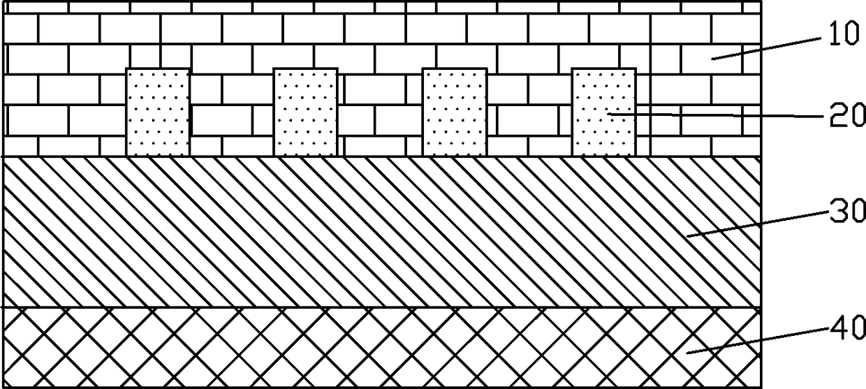
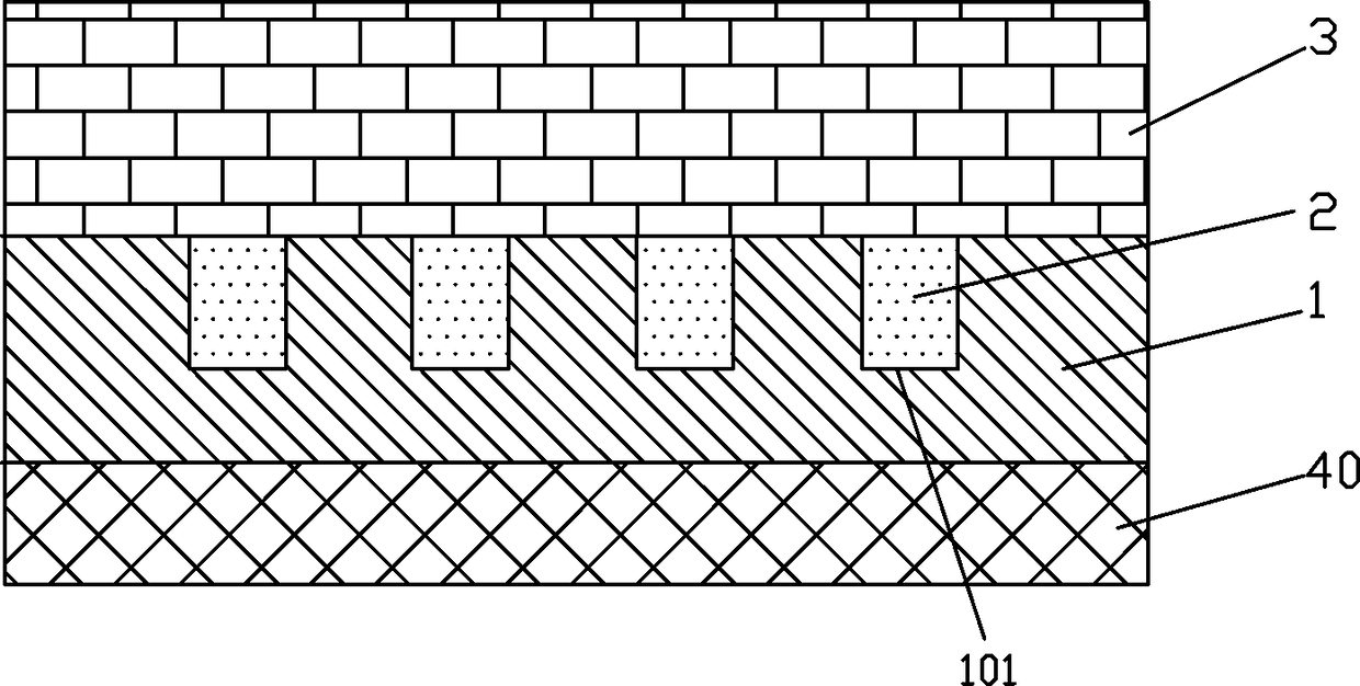
[0059] see figure 2 , the high-density optical waveguide structure of the present invention, which includes a lower cladding layer 1, a core layer 2, and an upper cladding layer 3; wherein, a plurality of grooves 101 are arranged at intervals in the lower cladding layer 1, and the grooves 101 are filled with light The waveguide material forms the core layer 2.

[0060] In this embodiment, the trench 101 is rectangular.

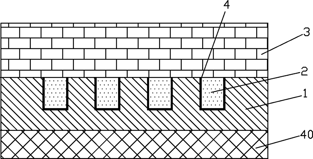
[0061] see image 3 , the inner wall of the groove 101 in the lower cladding layer 1 is provided with a reflective film 4, the thickness of the reflective film 4 is 0.1 nm-50 μm; the material of the reflective film 4 is polysiloxane.

[0062] see Figure 4 ~ Figure 7 , the longitudinal cross-sectional shape of the trench 101 in the lower cladding layer 1 is trapezoidal, circular, elliptical, or triangular.

[0063] Preferably, the optical waveguide material is acrylate, polymethyl methacrylate and its derivative fluoride, epoxy resin, fluorine-containing ...


PUM

PropertyMeasurementUnit
Thicknessaaaaaaaaaa

Abstract

The invention provides a high-density optical waveguide structure, a printing circuit board and a preparation method thereof. The high-density optical waveguide structure successively comprises a lower coating layer, a core layer and an upper coating layer; and a plurality of grooves are formed in the lower coating layer at intervals, and are filled with an optical waveguide materials to form thecore layer. Optical waveguide is integrated into a PCB to implement optoelectronic interconnection; high parallel interconnection density can be realized well, good signal integrity is maintained, andsizes of devices and equipment are reduced; meanwhile, power consumption is low, heat dissipation is facilitated, simple physical architecture and design can be realized, wiring space of the printingcircuit board is increased to a maximum extent, and manufacturing of an ultra-fine wire circuit board is facilitated; and moreover, wiring density of an existing preparation method can be improved, and the reliability is improved.

Description

technical field [0001] The invention relates to the manufacturing technology of a printed circuit board or a semiconductor integrated circuit packaging substrate, in particular to a high-density optical waveguide structure, a printed circuit board and a preparation method thereof. Background technique [0002] With the development of social economy, people's demand for information increases sharply, and the amount of information increases exponentially. Only the information bit rate that Internet users need to transmit increases by 8 times every year. In the field of long-distance wired communication, optical fiber communication technology can meet this high-performance requirement. However, in the field of short-distance information transmission, due to cost and technical issues, electrical interconnection is still the mainstay. However, electrical interconnection has inherent shortcomings such as electromagnetic interference, high loss, and low bandwidth, which limit the ...

Claims


Application Information

Patent Timeline
IPC IPC(8): G02B6/122H05K1/02H05K3/00
CPCG02B6/122G02B6/1221H05K1/0274H05K3/00
Inventor 石新红付海涛张军宗泽源周华梅朱龙秀梅莉嘉伊莫宁
Owner SHANGHAI MEADVILLE SCI & TECH
Why Eureka
Try Eureka