

A kind of oxide insulator thin film and thin film transistor
A thin film transistor and insulator technology, applied in the field of oxide insulator thin films and thin film transistors, can solve the problems of unfavorable electrical properties of oxide semiconductor devices, small Al ion radius, serious Al diffusion, etc., and achieve stable electrical properties of devices and breakdown field. Powerful, low water and oxygen permeability effect
- Summary
- Abstract
- Description
- Claims
- Application Information
AI Technical Summary
Problems solved by technology
Method used
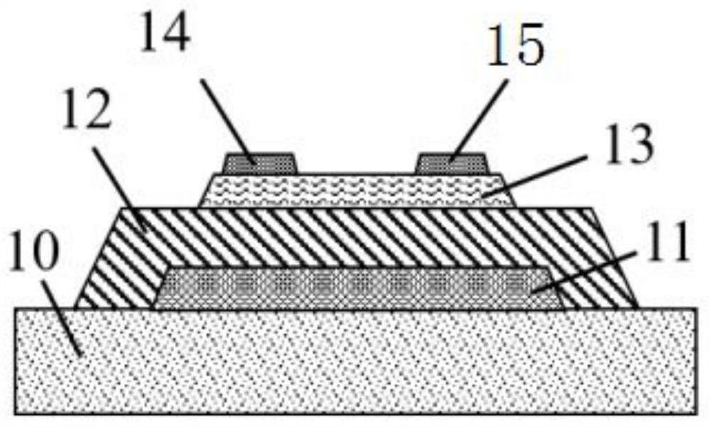
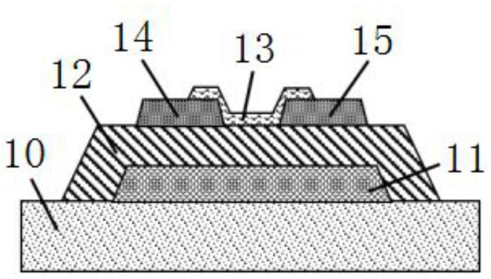
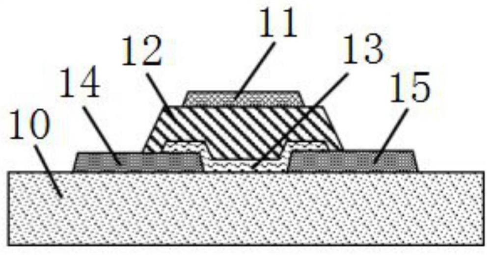
Image

Examples
Embodiment 1
[0029] An oxide insulator film, the composition of which is M x Al y Zr z o δ , M is a group IIIB metal element, 0.01≤x≤0.5, 0.3≤z<0.99, x+y+z=1, 0<δ≤2.
[0030] The film thickness is 2-1000nm. The thin film is prepared by vacuum method. Specifically, the vacuum method may be any one of single-target magnetron sputtering, multi-target magnetron sputtering, plasma-enhanced chemical vapor deposition, and atomic layer deposition.
[0031] The bandgap width of the film is greater than 4.5eV, which can effectively increase the injection barrier, and the breakdown field strength is greater than 3MV / cm, which can effectively reduce the breakdown probability. The thin film serves as an insulating layer for thin film transistors.
[0032] Compared with the traditional insulating film material, the M of the present embodiment x Al y Zr z o δ Oxide insulator thin films have the following excellent technical effects:
[0033] (1) The film still maintains an amorphous phase at a...
Embodiment 2
[0040] An oxide insulator thin film, the other features are the same as those in Embodiment 1, except that M is the element Sc or Y.
[0041] M in this example x Al y Zr z o δ In the oxide insulator film, M is the element Sc or Y. Since the oxide of Sc or Y has more negative fixed charges, it can shield part of the gate electric field, thereby offsetting the threshold voltage shift caused by the increase of carrier concentration. , which effectively avoids the problem of increased carrier concentration due to donor doping caused by the diffusion of Zr into oxide semiconductors (such as InZnO, InGaZnO, etc.).
Embodiment 3
[0043] An oxide insulator thin film, other features are the same as in Embodiment 2, the difference is that the thin film is prepared by a solution method, and the solution method is one of spin coating, scraping coating, spray coating and inkjet printing.
[0044]The oxide insulator thin film in this embodiment is prepared by a solution method. Compared with the vacuum method and other film preparation methods, the solution method has the advantages of low cost and easy control of the ratio. The solution method can simply adjust the composition of the precursor to control the ratio of the film components to achieve the control of the negative charge density in the insulating layer. Purpose, so that the threshold voltage of the thin film transistor can be adjusted more effectively.
PUM
| Property | Measurement | Unit |
|---|---|---|
| breakdown field strength | aaaaa | aaaaa |
| thickness | aaaaa | aaaaa |
| thickness | aaaaa | aaaaa |
Abstract
Description
Claims
Application Information