
A method for preparing high-performance nano-silver wire transparent conductive film by microwave welding

A technology of transparent conductive film and nano-silver wire, applied in the direction of equipment used to manufacture conductive/semiconductive layers, conductive materials dispersed in non-conductive inorganic materials, conductive layers on insulating carriers, etc., can solve the problem of affecting flexible display The electrical stability of the device, the reduction of the electrical properties of the transparent conductive film, and the degradation of the optical properties, etc., achieve the effects of excellent solvent wiping resistance, fast heating speed, and high reactivity

Active Publication Date: 2019-12-27
合肥微晶材料科技有限公司
View PDF5 Cites 0 Cited by
  • Summary
  • Abstract
  • Description
  • Claims
  • Application Information

AI Technical Summary

Problems solved by technology

[0003] At present, AgNWs are usually synthesized by polyol reduction method. During the synthesis process, polyvinylpyrrolidone (PVP) needs to be used as a stabilizer and guiding agent in the growth process of AgNWs, so a thin layer of PVP will remain on the surface of AgNWs, and PVP is used as an insulating layer. High contact resistance will be generated at the contact point of the conductive network of the transparent conductive film, thereby reducing the electrical properties of the transparent conductive film, and reducing the square resistance of the transparent conductive film by increasing the content of AgNWs will lead to a decrease in its optical properties and affect its display effect; At the same time, due to the point contact between the conductive networks, it affects the electrical stability of its application on flexible display devices.
[0004] Therefore, in view of the current problems such as high square resistance and poor stability of silver nano wire transparent conductive film, there is an urgent need for a method that has a simple preparation process, is suitable for industrial production, and has a small change to the original process to reduce the square resistance of nano silver wire transparent conductive film. Ways to improve the stability of its application

Method used


Image

  • A method for preparing high-performance nano-silver wire transparent conductive film by microwave welding
  • A method for preparing high-performance nano-silver wire transparent conductive film by microwave welding
  • A method for preparing high-performance nano-silver wire transparent conductive film by microwave welding

Examples


Embodiment 1

[0040] This embodiment prepares high-performance silver nano wire transparent conductive film according to the following steps:

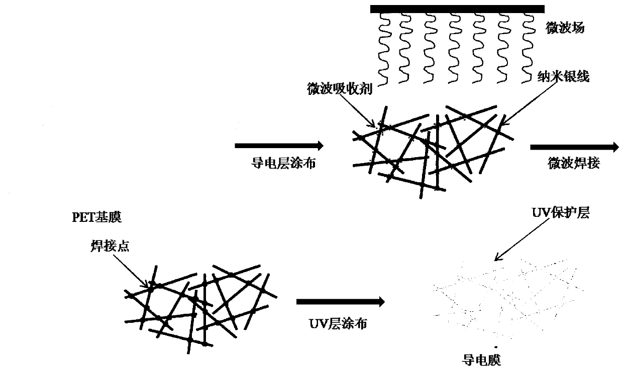
[0041] Step A, conductive layer coating

[0042] 3g of water-based polyester polyol ( Polyol HA-0135, Jiangshan Chemical), 7g water-based isocyanate curing agent Bayhydur 305 and 5000g deionized water were added to the dispersion tank, and mechanically stirred; then added 1.5g AgNWs (wire diameter 20nm, aspect ratio 1000- 2000, from Hefei Microcrystalline Material Technology Co., Ltd. (brand WJAG1, commercially available) and 30mg of nano-iron particles (5nm), continue to stir uniformly, and finally pass through a 800-mesh filter to prepare conductive ink;

[0043] Use dimple coating to uniformly coat the conductive ink on the non-hardened surface of the PET cured film, and then dry it in an IR oven at 120°C for 15s to form a conductive layer;

[0044] Step B. Microwave welding

[0045] Put the PET hardened film formed with a conductive layer in...

Embodiment 2

[0050] This embodiment prepares high-performance silver nano wire transparent conductive film according to the following steps:

[0051] Step A, conductive layer coating

[0052] 4g water-based polyester polyol ( Polyol HA-0135, Jiangshan Chemical), 9g water-based isocyanate curing agent Bayhydur 305 and 5000g deionized water were added to the dispersion tank, and mechanically stirred; then 2.5g AgNWs (wire diameter 20nm, aspect ratio 1000- 2000, from Hefei Microcrystalline Materials Technology Co., Ltd., brand WJAG1, available in the market) and 50mg of nano-iron particles (5nm), continue to stir uniformly, and finally pass through a 800-mesh filter to prepare conductive ink;

[0053] Use dimple coating to uniformly coat the conductive ink on the non-hardened surface of the PET cured film, and then dry it in an IR oven at 120°C for 15s to form a conductive layer;

[0054] Step B. Microwave welding

[0055] Put the PET hardened film formed with a conductive layer into a mi...

Embodiment 3

[0060] This embodiment prepares high-performance silver nano wire transparent conductive film according to the following steps:

[0061] Step A, conductive layer coating

[0062] 6g water-based polyester polyol ( Polyol HA-0135, Jiangshan Chemical), 14g water-based isocyanate curing agent Bayhydur XP 2655 and 5000g deionized water are added to the dispersion tank, mechanically stirred; then add 1.5g AgNWs (wire diameter 20nm, aspect ratio 1000) while stirring -2000, from Hefei Microcrystalline Materials Technology Co., Ltd., brand WJAG1, available in the market) and 30mg nano-chromium particles (7nm), continue to stir uniformly, and finally pass through a 800-mesh filter screen to obtain conductive ink;

[0063] Use dimple coating to uniformly coat the conductive ink on the non-hardened surface of the PET cured film, and then dry it in an IR oven at 120°C for 15s to form a conductive layer;

[0064] Step B. Microwave welding

[0065] Put the PET hardened film formed with a...


PUM

PropertyMeasurementUnit
particle diameteraaaaaaaaaa
diameteraaaaaaaaaa
wavelengthaaaaaaaaaa

Abstract

The invention discloses a method for making high performance nanometer silver wire transparent electric conduction membrane via microwave joining. The method comprises the following steps: a microwaveabsorbent is added into an electric conduction ink; during electric conduction layer coating operation, the microwave absorbent is adsorbed at nodes of an electric conduction network in a concentrated manner and is enabled to reach a stable state; rapid heating of the microwave absorbent is realized and welding operation is finished during microwave joining operation, other areas of the electricconduction network cannot be affected, a UV protection layer is coated on a surface of the electric conduction layer, and a formed transparent electric conduction membrane is enabled to be high in weatherability. The nanometer silver wire transparent electric conduction membrane formed via the method disclosed in the invention is excellent in sheet resistivity which can be as low as 5 ohms, optical performance is improved due to a low usage quantity of nano silver, the membrane is greater than 90% in light transmittance and lower than 0.7 in haze, the membrane is also excellent in bending resistance and is as low as 1 mm in bending diameter, bending resistant frequency is greater than 100 thousand, and excellent weatherability is also realized.

Description

technical field [0001] The invention relates to the field of display, in particular to a method for preparing a silver nano wire transparent conductive film with high optical performance, low square resistance and high stability. The transparent conductive film prepared by the method is suitable for use in flexible displays and large-scale devices superior. Background technique [0002] As one of the key components in the fields of display and thin-film solar energy, transparent conductive film is currently the most widely used transparent conductive film of indium tin oxide (ITO). However, with the gradual increase in the size of product requirements, the increase in the demand for flexible displays, and the increase in the use of transparent conductive films, ITO has some insurmountable problems, such as high square resistance, low sensitivity, and flexible substrates. Fragile, shortage of indium resources, etc. In order to overcome the problems existing in ITO, in recen...

Claims


Application Information

Patent Timeline
Patent Type & Authority Patents(China)
IPC IPC(8): H01B5/14H01B1/22H01B13/00
CPCH01B1/22H01B5/14H01B13/0026
Inventor 吕鹏张梓晗杨锦张运奇聂彪
Owner 合肥微晶材料科技有限公司
Learn More