Efficient high-temperature curing technology of silicon carbide seed crystals

A technology of high-temperature solidification and silicon carbide, which is applied in the direction of single crystal growth, crystal growth, single crystal growth, etc., can solve the problems affecting the quality of crystal growth and general fixation effect, and achieve good fixation effect, good fixation and complete graphitization Effect

Active Publication Date: 2018-08-31
FUJIAN NORSTEL MATERIAL TECH CO LTD
View PDF4 Cites 4 Cited by
  • Summary
  • Abstract
  • Description
  • Claims
  • Application Information

AI Technical Summary

Problems solved by technology

However, the seed crystal fixing method used in this patent for silicon carbide crystal growth is to coat the reverse side of the seed crystal gro

Method used


Image

  • Efficient high-temperature curing technology of silicon carbide seed crystals
  • Efficient high-temperature curing technology of silicon carbide seed crystals

Examples


Embodiment 1

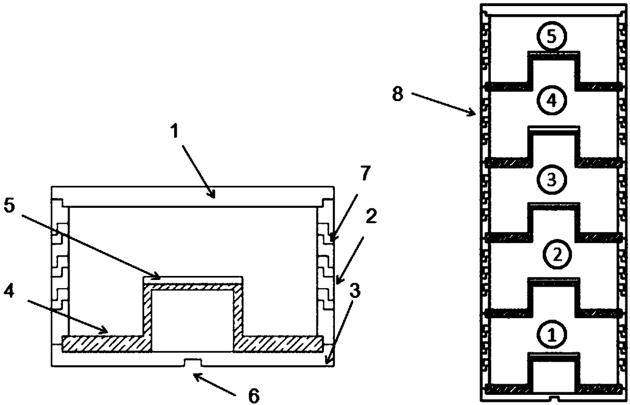
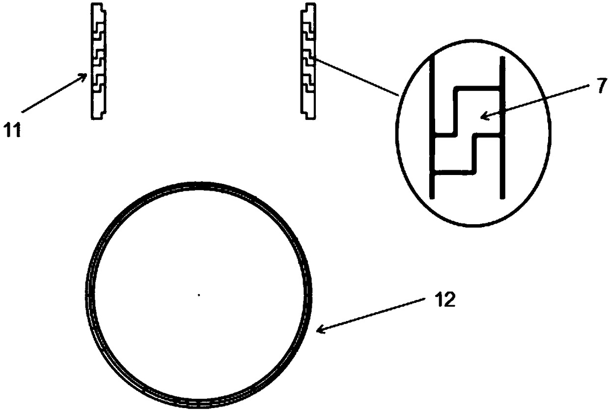
[0042] A process for high-efficiency high-temperature solidification of silicon carbide seed crystals, using a crucible fixture with a cover, a crucible cover, a crucible with a thickness of 10mm, a chassis, a temperature measurement hole on the chassis with a diameter of 5mm, and a vent hole for high-temperature solidification of silicon carbide seed crystals ; Every two adjacent air holes with a diameter of 10mm form an inverted Z shape, the central axes of the two holes are respectively inclined at 5° from the horizontal line, and the central axes of the inner and outer holes are 1 / 4 of the air hole diameter apart, and they meet and overlap at the center of the crucible wall The intersection and conduction at the intersection, wherein the inner hole is at a high position; the crucible fixture is made of graphite material; the temperature measurement hole of the chassis is measured and controlled by an infrared pyrometer; the following steps are included:

[0043] Step S1, pa...

Embodiment 2

[0052] A process for high-efficiency high-temperature solidification of silicon carbide seed crystals, using a crucible fixture with a cover, a crucible cover, a crucible with a thickness of 30 mm, a chassis, a temperature measurement hole on the chassis with a diameter of 20 mm, and a vent hole for high-temperature solidification of silicon carbide seed crystals ; Each two adjacent air holes with a diameter of 30mm form an inverted Z-shape, the central axes of the two holes are respectively inclined at 15° from the horizontal line, and the central axes of the inner and outer holes are 1 / 4 of the air hole diameter apart, and they meet and overlap at the center of the crucible wall The intersection and conduction at the intersection, wherein the inner hole is at a high position; the crucible fixture is made of graphite material; the temperature measurement hole of the chassis is measured and controlled by an infrared pyrometer; the following steps are included:

[0053] Step S1,...

Embodiment 3

[0062] A process for high-efficiency high-temperature solidification of silicon carbide seed crystals, using a crucible fixture with a lid, a crucible cover, a crucible with a thickness of 20mm, a chassis, a chassis temperature measuring hole with a diameter of 12.5mm, and a vent hole for high temperature silicon carbide seed crystals Solidification; every two adjacent air holes with a diameter of 20mm form an inverted Z-shape, the central axes of the two holes are respectively inclined at 10° from the horizontal line, and the central axes of the inner and outer holes are 1 / 4 of the air hole diameter apart, and meet at the center of the crucible wall The overlaps meet and conduct, and the inner hole is at a high position; the crucible fixture is made of graphite material; the temperature measurement hole of the chassis is measured and controlled by an infrared pyrometer; the following steps are included:

[0063] Step S1, paste the silicon carbide seed crystal on the crucible c...


PUM

PropertyMeasurementUnit
Thicknessaaaaaaaaaa
Diameteraaaaaaaaaa
Thicknessaaaaaaaaaa

Abstract

The invention discloses an efficient high-temperature curing technology of silicon carbide seed crystals. The technology is characterized in that the silicon carbide seed crystals are cured under hightemperature through a crucible jig which is provided with a cover, a crucible cover, a crucible, a chassis, a chassis temperature measuring hole and an air hole; every two adjacent air holes of the air holes form an inverted Z shape; intermediate axes of the two holes are correspondingly inclined by 5-15 degrees relative to a horizontal line and are intersected and connected in the center of thecrucible wall. The method comprises the following steps: adhering the silicon carbide seed crystals to the crucible cover through a carbon-rich adhering agent; sequentially overlapping the crucible and the crucible cover adhered with the seed crystals from the chassis; closing the cover; transferring the crucible jig into a high-temperature furnace; vacuumizing the crucible jig; charging argon into the crucible jig; heating the crucible jig through a water cooling type induction coil or a resistor; and graphitizing carbon paste to realize efficient high temperature curing of the silicon carbide seed crystals. With the adoption of the technology, the seed crystals can be greatly adhered and completely cured; the defects are small; and the subsequent crystal growing quality is high.

Description

technical field [0001] The invention relates to the technical field of single crystal growth, in particular to a process for high-efficiency high-temperature solidification of silicon carbide seed crystals. Background technique [0002] Silicon carbide single crystal material is one of the third-generation semiconductor materials that can not only meet the ideal substrate material for manufacturing high-brightness gallium nitride light emitting and laser diodes, but also meet the requirements for manufacturing semiconductor integrated circuits and devices. Silicon carbide single crystal materials have the characteristics of wide bandgap, high thermal conductivity, high breakdown electric field, and high radiation resistance, making them widely used in artificial satellites, rockets, radar and communications, aerospace vehicles, marine exploration, earthquake prediction, petroleum It has a wide range of applications in important fields such as drilling, machining, and automot...

Claims


Application Information

Patent Timeline
IPC IPC(8): C30B29/36C30B23/00
CPCC30B23/00C30B29/36
Inventor 陈华荣张洁廖弘基蔡如腾
Owner FUJIAN NORSTEL MATERIAL TECH CO LTD
Why Eureka
Try Eureka