Single crystal growth method for ferromagnetic semiconductor material

A growth method, semiconductor technology, applied in the direction of single crystal growth, single crystal growth, polycrystalline material growth, etc., can solve the problems of limited chemical solubility, carrier and spin can not be adjusted separately

Active Publication Date: 2018-09-07
INST OF PHYSICS - CHINESE ACAD OF SCI
View PDF4 Cites 1 Cited by
  • Summary
  • Abstract
  • Description
  • Claims
  • Application Information

AI Technical Summary

Problems solved by technology

For example by Mn 2+ replace Ga 3+ (Ga,Mn)As and (Ga,Mn)N, due to unequal substitution, lead to very limited chemical solubility, can only be prepared in the form of epitaxial thin films, and the carriers and spins cannot be adjusted separately (H . Ohno, et al., Science 281, 951-956 (1998))

Method used


Image

  • Single crystal growth method for ferromagnetic semiconductor material
  • Single crystal growth method for ferromagnetic semiconductor material
  • Single crystal growth method for ferromagnetic semiconductor material

Examples


Embodiment 1

[0051] (1) In a glove box filled with argon gas, Zn powder, Mn powder and As powder were uniformly mixed according to the molar ratio of 5.8:0.2:6, and pressed into small discs. Then weigh Ba block and K block according to the mol ratio of Ba:K:Zn:Mn:As=0.95:0.05:5.4:0.6:6 (total mass is about 5g), and Zn powder, Mn powder and As powder The mixture disk is put into the alumina ceramic test tube together with the Ba block and the K block;

[0052] (2) Vacuum seal the ceramic test tube with the raw material in the quartz tube, then fill the quartz tube with argon gas of 0.2 Bar and seal it;

[0053] (3) The sealed quartz tube was sintered in a high-temperature furnace at 1000°C for 30 hours, and then cooled to 500°C at a rate of 5°C / hour.

[0054] (4) obtained after dissociation (Ba 0.95 K 0.05 )(Zn 0.9 mn 0.1 ) 2 As 2 Diluted magnetic semiconductor single crystal.

[0055] Product Characterization:

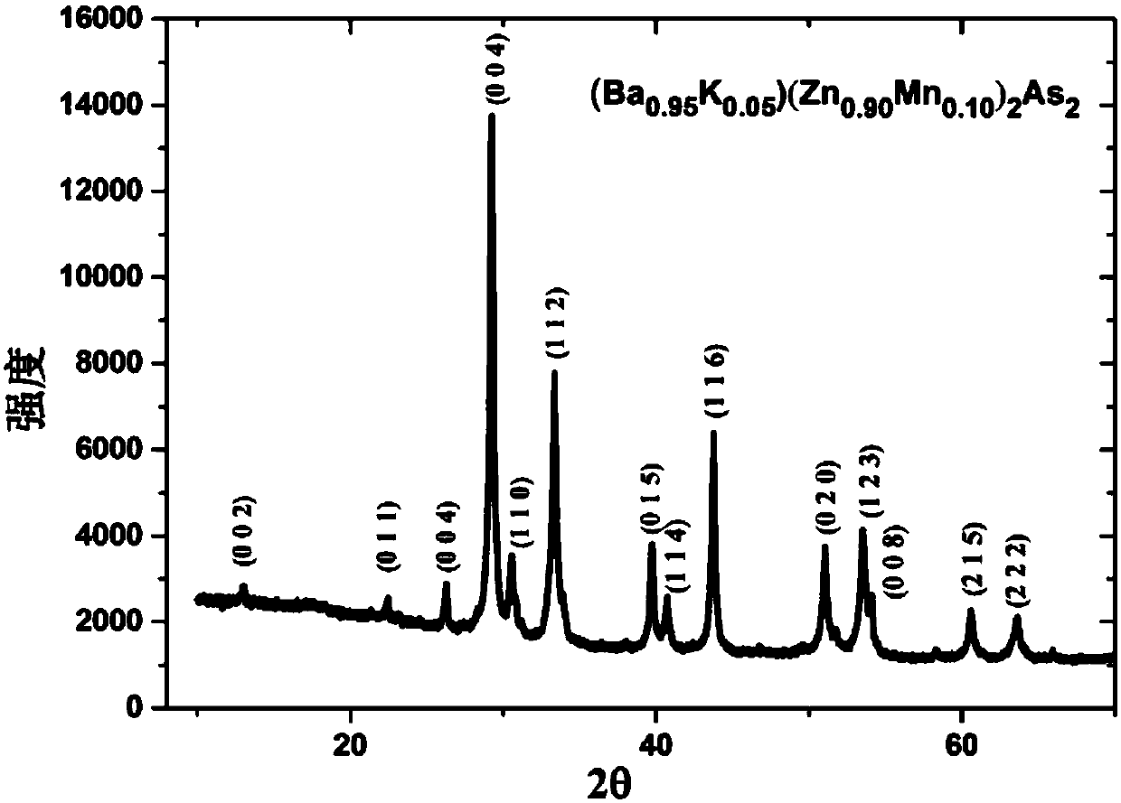
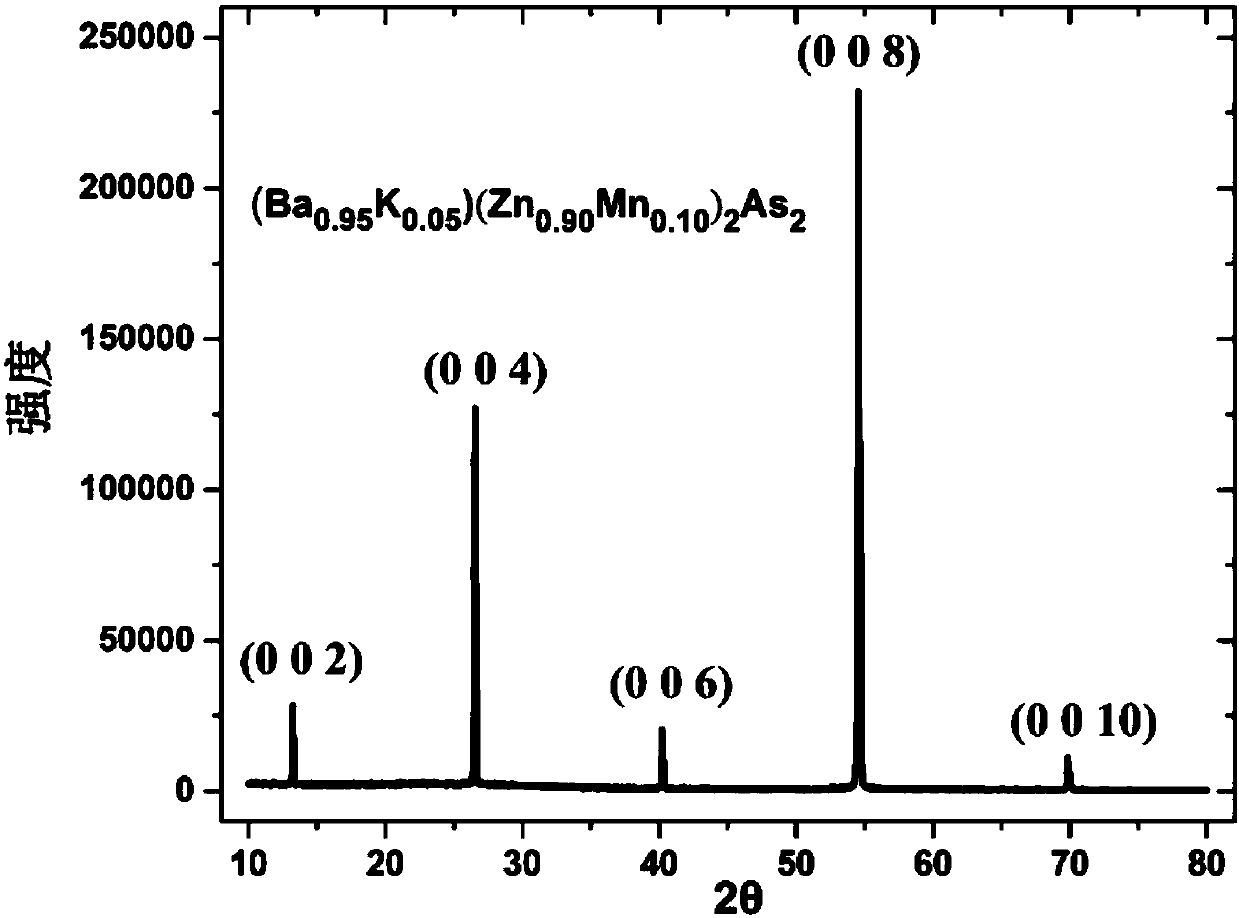
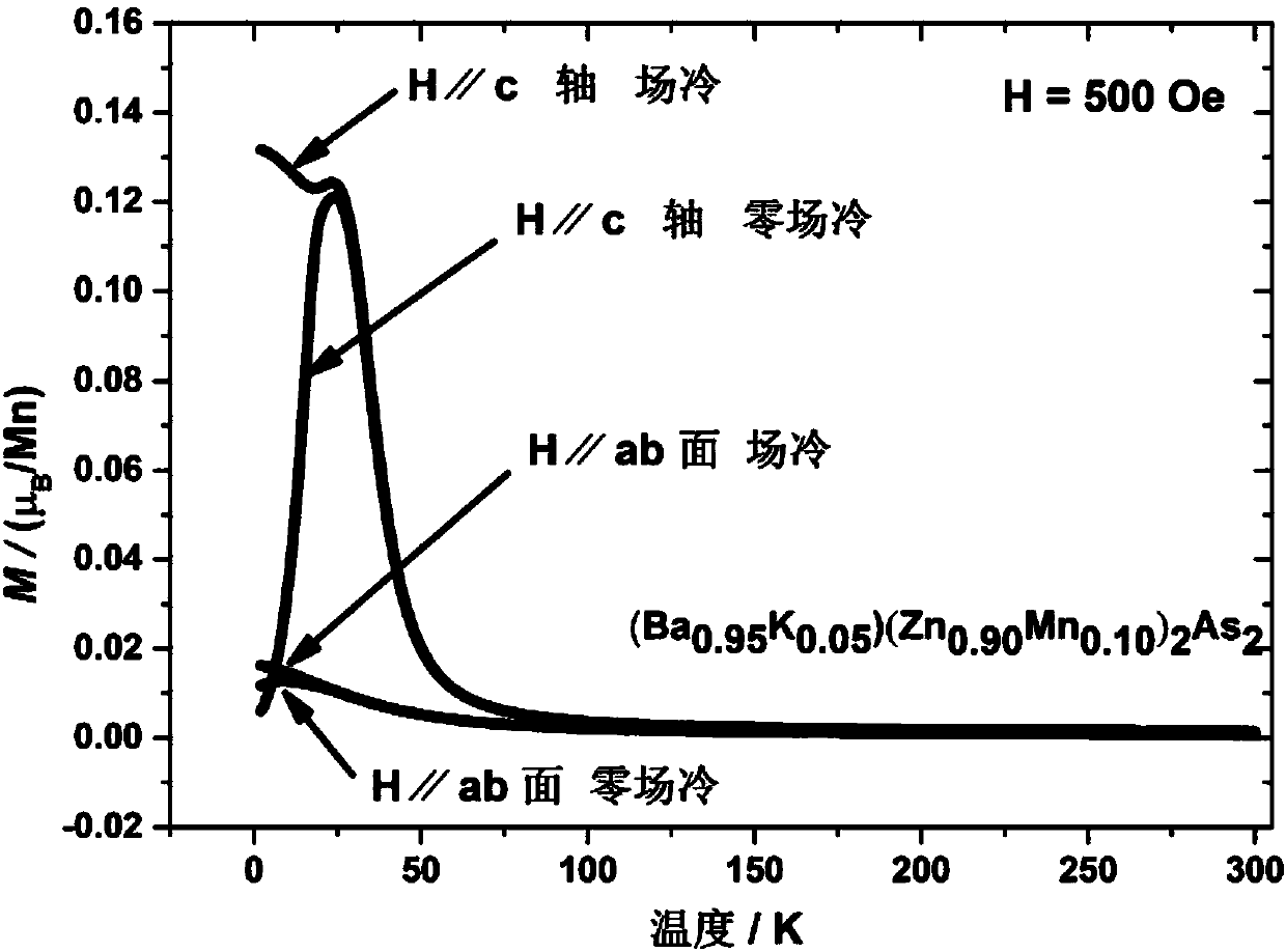
[0056] 1. The single crystal powder obtained in this example is gro...

Embodiment 2

[0062] (1) Weigh BaAs, KAs, Zn, Mn and As (total mass is About 10g), put into the alumina ceramic test tube;

[0063] (2) Vacuum seal the ceramic test tube with the raw material in the quartz tube, then fill the quartz tube with argon gas of 0.2 Bar and seal it;

[0064] (3) Sinter the sealed quartz tube in a high-temperature furnace at 1300°C for 10 hours, and then cool it down to 500°C at a rate of 1°C / hour

[0065] (4) obtained after dissociation (Ba 0.5 K 0.5 )(Zn 0.95 mn 0.05 ) 2 As 2 Diluted magnetic semiconductor single crystal.

[0066] Product Characterization:

[0067] 1. The single crystal powder obtained in this example is ground and subjected to a powder X-ray diffraction experiment. The diffraction spectrum is as follows: Figure 7 As shown; the single wafer is directly scanned in the θ-2θ mode, that is, the powder X-ray diffraction mode, and the diffraction spectrum is obtained as Figure 8 shown. Figure 7 All the peaks in all come from the product...

Embodiment 3

[0073] (1) Weigh Zn powder, Mn powder, As powder, BaAs powder and KAs powder according to the mol ratio of Ba:K:Zn:Mn:As=0.85:0.15:2.4:1.6:4 in the argon glove box (The total mass is about 1g);

[0074] (2) Put the above raw materials into tantalum foil or gold foil, and pre-press into cylinder, and then packaged into a Φ8×15mm BN tube;

[0075] (3) Put the BN tube into a graphite furnace and put it into a high-pressure assembly for high-pressure synthesis. The sample synthesis is carried out on a large six-sided top press. Before the high-pressure experiment, the temperature and pressure are first calibrated, and the heating temperature is controlled by controlling the heating power. First slowly increase the pressure to 1GPa at room temperature, then start the heating program to heat up to 1150°C, then sinter at 1150°C for 3 hours, and then cool down to 700°C at a rate of 1°C / min.

[0076] (4) obtained after dissociation (Ba 0.85 K 0.15 )(Zn 0.6 mn 0.4 ) 2 As 2Dilu...


PUM


Abstract

The invention provides a single crystal growth method for a ferromagnetic semiconductor material. The ferromagnetic semiconductor material has a chemical formula of (Ba<1-x>K<x>)(Zn<1-y>Mn<y>)<2>As<2>, wherein x is more than 0 and less than 0.5, and y is more than 0 and less than 0.5. The single crystal growth method comprises a step of growing single crystals by using a flux process under heatingconditions, wherein fluxes used in the method are ZnAs and MnAs. The method of the invention is capable of growing large-size high-quality (Ba,K) (Zn,Mn)<2>As<2> single crystals, which is of important significance to research on the physical mechanisms of the crystal and practical application of the crystal in the future.

Description

technical field [0001] The invention relates to a ferromagnetic semiconductor material (Ba, K) (Zn, Mn) 2 As 2 method for growing large-scale single crystals. Background technique [0002] Diluted magnetic semiconductor materials have attracted extensive attention due to their potential applications in the field of spintronic devices. Diluted magnetic semiconductors are generally obtained by introducing a small amount of magnetic ions into the semiconductor. Typical are III-V based semiconductors. For example by Mn 2+ replace Ga 3+ (Ga,Mn)As and (Ga,Mn)N, due to unequal substitution, lead to very limited chemical solubility, can only be prepared in the form of epitaxial thin films, and the carriers and spins cannot be adjusted separately (H . Ohno, et al., Science 281, 951-956 (1998)). Recently, based on II-II-V semiconductor BaZn 2 As 2 The dilute magnetic semiconductor (Ba,K)(Zn,Mn) 2 As 2 was successfully prepared (K.Zhao et al., Nature Communications 4:1442(20...

Claims


Application Information

Patent Timeline
Patent Type & Authority Applications(China)
IPC IPC(8): C30B9/12C30B29/10H01F1/40H01F41/00
CPCC30B9/12C30B29/10H01F1/401H01F41/00
Inventor 靳常青赵国强邓正
Owner INST OF PHYSICS - CHINESE ACAD OF SCI
Why Eureka
Try Eureka