A kind of manufacturing method of igbt chip with compound gate structure containing dummy gate

A manufacturing method and compound gate technology, which are applied in semiconductor/solid-state device manufacturing, semiconductor devices, electrical components, etc., to achieve the effect of shielding mutual interference, retaining low power consumption, and solving high-voltage state voltage drop

Active Publication Date: 2020-11-10
ZHUZHOU CRRC TIMES SEMICON CO LTD
View PDF4 Cites 0 Cited by
  • Summary
  • Abstract
  • Description
  • Claims
  • Application Information

AI Technical Summary

Problems solved by technology

[0006] figure 2 and image 3 The bottom of the trench gate has a certain limit on the resistance capacity of the IGBT chip
its with figure 1 Compared with the IGBT chip with a planar gate structure shown in the figure, while improving the performance of the IGBT chip, it also sacrifices part of the withstand voltage and solid performance of the planar gate.

Method used


Image

  • A kind of manufacturing method of igbt chip with compound gate structure containing dummy gate
  • A kind of manufacturing method of igbt chip with compound gate structure containing dummy gate
  • A kind of manufacturing method of igbt chip with compound gate structure containing dummy gate

Examples


Embodiment Construction

[0048] The implementation of the present invention will be described in detail below in conjunction with the accompanying drawings and examples, so as to fully understand and implement the process of how to apply technical means to solve technical problems and achieve technical effects in the present invention. It should be noted that, as long as there is no conflict, each embodiment and each feature in each embodiment of the present invention can be combined with each other, and the formed technical solutions are all within the protection scope of the present invention.

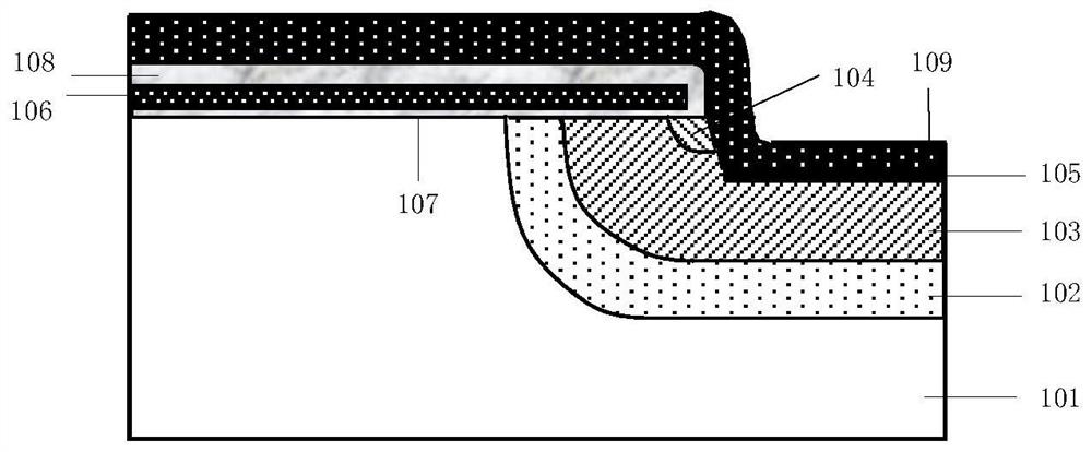
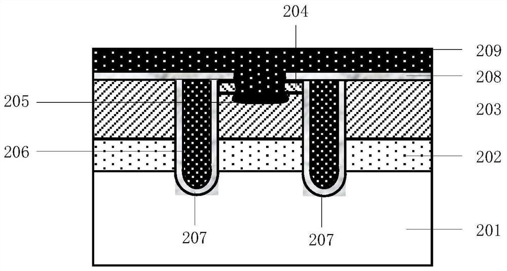
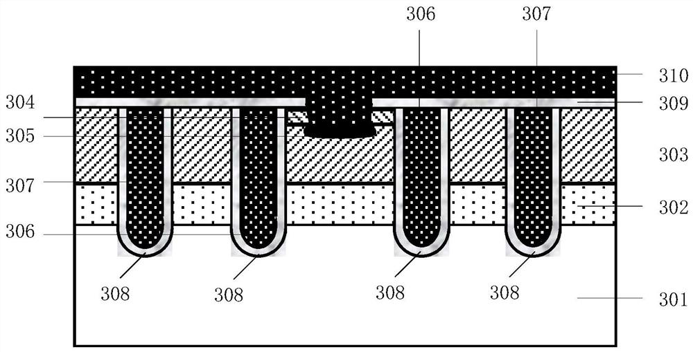
[0049] In this embodiment, the IGBT chip includes multiple cells, such as Figure 4 As shown, each cell 410 may be a hexagonal cell structure, and a plurality of cells 410 are distributed on the wafer substrate in a honeycomb shape. Moreover, each cell 410 includes a gate region 401 , and trench gate active regions 402 and planar gate active regions 403 located on both sides of the gate region 401 .

[0050...


PUM

PropertyMeasurementUnit
thicknessaaaaaaaaaa
thicknessaaaaaaaaaa
thicknessaaaaaaaaaa

Abstract

The invention discloses a manufacturing method of an IGBT chip with a composite gate structure containing a virtual gate; the method comprises the following steps: etching on a wafer substrate to formadjacent first and second grooves, forming a second groove gate in the second groove to serve as the virtual gate, and forming a first groove gate and a planar gate connected via a polysilicon; the virtual gate is arranged between the first groove gate and the planar gate, and separated from the two via an oxide layer; a N well zone, a P well zone, a P+ doped zone and a N+ doped diffusion zone distributed from bottom to top in a groove gate active region and a planar gate active region are respectively formed via a same process. The planar gate and the groove gate coexist on the same chip, thus greatly improving the chip density; the virtual gate is suspended or grounded so as to effectively shield the mutual interferences between the planar gate structure and the groove gate structure, thus optimizing input and output capacitance of the composite gate, optimizing the chip opening speed, and reducing switching losses.

Description

technical field [0001] The invention relates to the technical field of manufacturing semiconductor devices, in particular to a method for manufacturing an IGBT chip with a composite gate structure including a dummy gate. Background technique [0002] Since the advent of IGBT (Insulated Gate Bipolar Transistor, Insulated Gate Bipolar Transistor) devices around 1980, due to the characteristics of bipolar transistor on-state voltage drop and high current density, and MOSFET (Metal-Oxide-Semiconductor Field -Effect Transistor, Metal-Oxide Semiconductor Field Effect Transistor) has high input impedance and fast response, and is widely used in rail transit, smart grid, industrial frequency conversion and new energy development and other fields. [0003] figure 1 It is a schematic cross-sectional view of a half cell of an IGBT chip with a planar gate structure in the prior art. Such as figure 1 As shown, it mainly includes: wafer substrate 101, N well region 102, P well region 1...

Claims


Application Information

Patent Timeline
Patent Type & Authority Patents(China)
IPC IPC(8): H01L29/739H01L21/331
CPCH01L29/66348H01L29/7397
Inventor 刘国友朱春林朱利恒
Owner ZHUZHOU CRRC TIMES SEMICON CO LTD
Why Eureka
Try Eureka