
CMOS rear end technology-embedded ferroelectric random memory and preparation method thereof

A technology of random access memory and back-end technology, applied in capacitors, electric solid-state devices, circuits, etc., can solve problems such as difficult to meet, low thermal budget, poor electrical performance of PZT film, etc., achieve low process cost, reduce manufacturing cost, high memory effect of density

Inactive Publication Date: 2018-09-11
XIANGTAN UNIV
View PDF4 Cites 8 Cited by
  • Summary
  • Abstract
  • Description
  • Claims
  • Application Information

AI Technical Summary

Problems solved by technology

However, the electrical properties of PZT thin films prepared by low-temperature processes (less than 600°C) are poor; on the other hand, as the process size continues to shrink, this technology is also difficult to meet the lower and lower thermal budgets.

Method used


Image

  • CMOS rear end technology-embedded ferroelectric random memory and preparation method thereof
  • CMOS rear end technology-embedded ferroelectric random memory and preparation method thereof
  • CMOS rear end technology-embedded ferroelectric random memory and preparation method thereof

Examples


Embodiment Construction

[0043] In order to make the above objects, features and advantages of the present invention more comprehensible, specific implementations of the present invention will be described in detail below in conjunction with the accompanying drawings.

[0044] Many specific details are set forth in the following description to fully understand the present invention, but based on the current rapid development of CMOS silicon process technology, the present invention can also be implemented in other ways than those described here. The present invention mainly proposes an idea of ​​embedding and integrating a ferroelectric capacitor on a CMOS process line, and its inventive point is not limited to the replacement and change of a certain specific process.

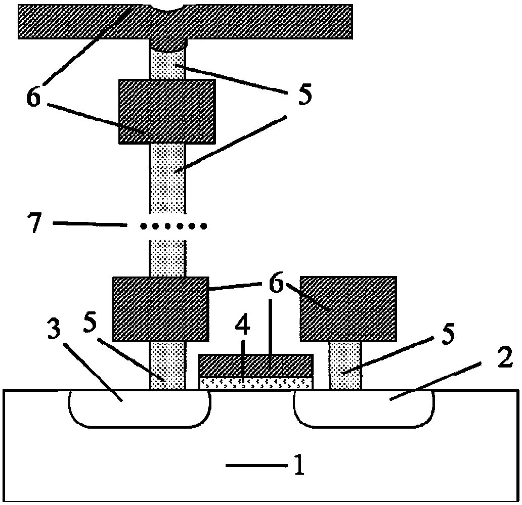
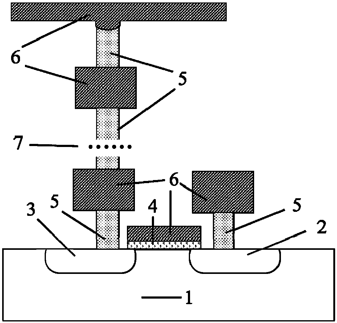
[0045] refer to figure 2 The source region (2), the drain region (3), the gate dielectric layer (4), the through hole (5), and the necessary metal interconnection (6, 7) of the transistor are completed on the traditional CMOS process ...


PUM

PropertyMeasurementUnit
Thicknessaaaaaaaaaa

Abstract

The invention provides a CMOS rear end technology-embedded ferroelectric random access memory with high storage density and low process cost and a preparation method thereof. The characteristics of the low-temperature annealing process of the new ferroelectric material hafnium oxide or zirconia are used and the appropriate upper and lower metal electrodes are combined, so that a capacitor is integrated into the CMOS rear end process line to realize information storage and reading. In addition, the present invention also discloses a preparation method for preparing a ferroelectric memory whichis fully compatible with a 0.13 [mu]m CMOS process line, does not require a special barrier layer and packaging technology, and has good radiation resistance.

Description

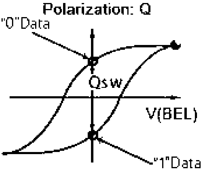
technical field [0001] The invention belongs to the technical field of integrated circuit technology, relates to the field of integrated technology of novel memories, in particular to a CMOS-compatible, embedded ferroelectric random access memory (FRAM) and a preparation method thereof. Background technique [0002] FRAM is a very promising class of next-generation memory technology and has been the focus of attention. It integrates ferroelectric capacitors (including bottom electrodes, ferroelectric thin film materials and top electrodes) into complementary oxide metal semiconductors (CMOS), and defines the positive and negative polarized charge values ​​​​on the hysteresis loop of ferroelectric capacitors as data" 0" and "1" to realize the storage function, such as figure 1 . FRAM has the characteristics of both RAM (random access memory) and ROM (read-only memory). It has advantages in non-volatility, low power consumption, fatigue resistance, fast read and write speed,...

Claims


Application Information

Patent Timeline
IPC IPC(8): H01L27/11507H01L27/11509H01L49/02
CPCH01L28/40H10B53/30H10B53/40
Inventor 廖佳佳彭强祥曾斌建廖敏周益春
Owner XIANGTAN UNIV
Learn More