Hidden cutting LED chip and manufacturing method thereof

A LED chip and invisible cutting technology, which is applied in semiconductor/solid-state device manufacturing, electrical components, circuits, etc., can solve problems such as inability to split, poor splitting, and low output rate, so as to facilitate mass production and improve Fragment yield rate, the effect of solving the leakage problem

Pending Publication Date: 2018-09-14
FOSHAN NATIONSTAR SEMICON
View PDF4 Cites 4 Cited by
  • Summary
  • Abstract
  • Description
  • Claims
  • Application Information

AI Technical Summary

Problems solved by technology

This method is prone to two adverse consequences: 1) a large number of fragments appear, the fragmentation rate is high, and the output rate is low; 2) it cannot be split, or the split is poor, and the yield rate is low
[0007] Chinese patent document CN103000507B discloses a manufacturing method for improving brightness and yield of medium and large-sized chips. It specifically discloses a cutting process that adopts invisible cutting on the back and has a cutting depth greater than 1 / 2 of the thickness of the chip, which solves the problem of oblique cracks. Low yield rate, low brightness and other technical problems
If this method is applied to sapphire substrates, it will consume a lot of diamond cutters, the efficiency is low, and appearance problems such as edge chipping, oblique cracks, and twin crystals will easily occur after cutting.

Method used


Image

  • Hidden cutting LED chip and manufacturing method thereof
  • Hidden cutting LED chip and manufacturing method thereof
  • Hidden cutting LED chip and manufacturing method thereof

Examples


Embodiment Construction

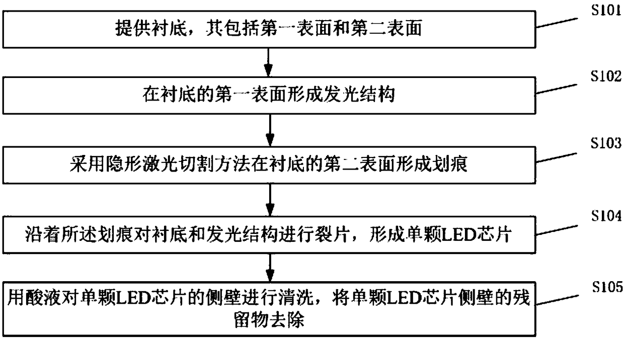
[0037] In order to make the object, technical solution and advantages of the present invention clearer, the present invention will be further described in detail below in conjunction with the accompanying drawings.

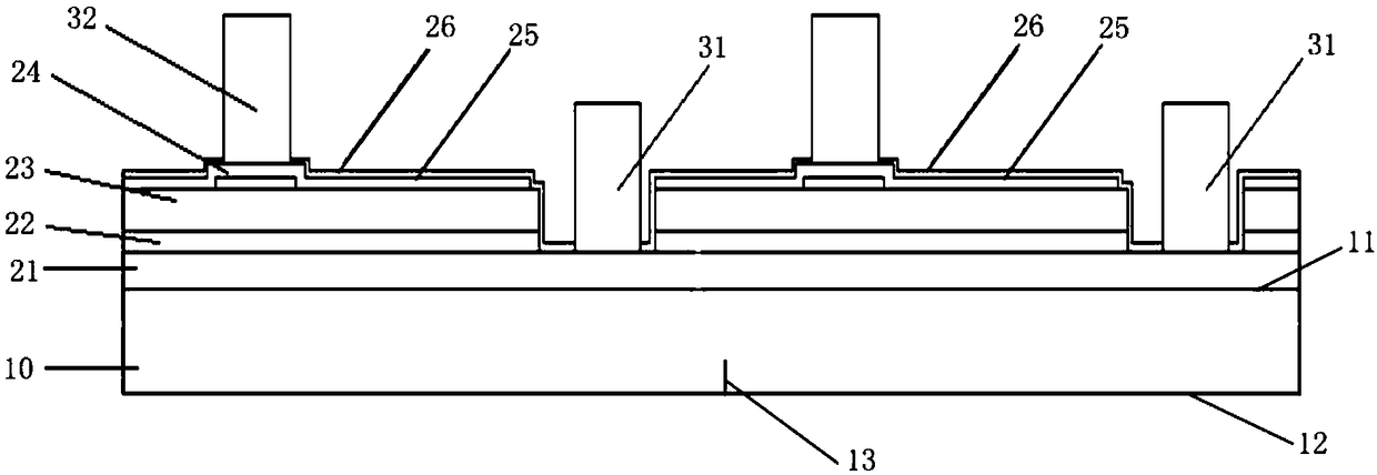
[0038] see figure 1 , a stealth-cut LED chip provided by the present invention includes a substrate 10, which includes a first surface 11 and a second surface 12, a light-emitting structure arranged on the first surface 11 of the substrate 10, and a light-emitting structure arranged on the second surface of the substrate 10. Scratches 13 on the surface 12 , the depth of the scratches 13 is greater than one-fifth of the thickness of the substrate 10 and less than one-third of the thickness of the substrate 10 .

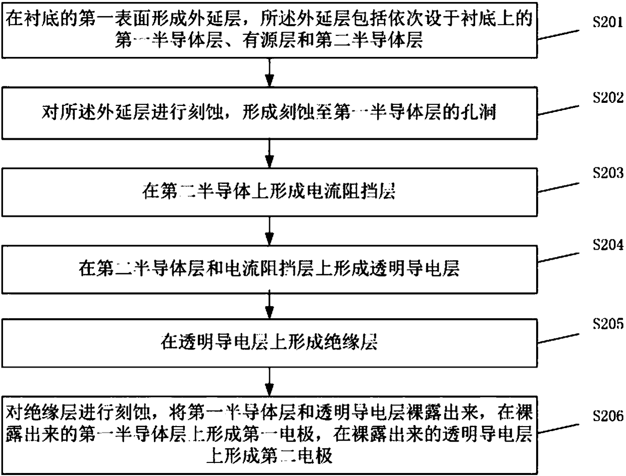
[0039] The material of the substrate 10 may be sapphire, silicon carbide or silicon, or other semiconductor materials. The substrate in this embodiment is preferably a sapphire substrate. The first surface 11 and the second surface 12 of the substrate 10 ...


PUM


Abstract

The present invention discloses a hidden cutting LED chip and a manufacturing method thereof. The manufacturing method comprises the steps of: providing a substrate consisting of a first surface and asecond surface; forming a luminescence structure at the first surface of the substrate; employing a hidden laser cutting method to form scratches at the second surface of the substrate; performing splitting of the substrate and the luminescence structure along the scratches to form a single LED chip; and performing cleaning of the side walls of the single LED chip by employing acid liquor, and removing the residue at the side walls of the single LED chip. The hidden cutting LED chip and the manufacturing method thereof effectively solve the electric leakage problem of a LED chip without cutting channels, improve the chip yield and are convenient for large-scale mass production.

Description

technical field [0001] The invention relates to the technical field of light-emitting diodes, in particular to a stealth-cut LED chip and a manufacturing method thereof. Background technique [0002] LED (Light Emitting Diode, Light Emitting Diode) is a semiconductor device that uses carrier recombination to release energy to form light. The formal LED chip has low power consumption, pure chromaticity, long life, small size, fast response time, energy saving and environmental protection. and many other advantages. [0003] Traditional chip cutting methods such as diamond scribing and grinding wheel sawing have gradually become outdated due to their low efficiency and low yield, and cannot meet the needs of modern production. At present, laser cutting is gradually replacing traditional cutting and becoming the current mainstream cutting method. Laser cutting is divided into surface cutting and internal cutting, that is, invisible cutting. Laser scribing is a new type of cut...

Claims


Application Information

Patent Timeline
Patent Type & Authority Applications(China)
IPC IPC(8): H01L21/78H01L21/304H01L33/00
CPCH01L21/78H01L21/304H01L33/00
Inventor 崔永进
Owner FOSHAN NATIONSTAR SEMICON
Why Eureka
Try Eureka