Gallium nitride Schottky barrier diode and manufacturing method thereof

A technology of Schottky potential and manufacturing method, which is applied in semiconductor/solid-state device manufacturing, semiconductor devices, electrical components, etc., can solve problems affecting the efficiency of rectification systems, large reverse leakage current, and insufficient stability of diodes, etc., to achieve Effects of low leakage current, reduced reverse leakage current, and high stability

Inactive Publication Date: 2018-09-18
江西誉鸿锦芯片科技有限公司
View PDF5 Cites 6 Cited by
  • Summary
  • Abstract
  • Description
  • Claims
  • Application Information

AI Technical Summary

Problems solved by technology

[0003] The purpose of the present invention is to provide a Gallium Nitride Schottky barrier diode and its manufacturing method, which solves the problem that the stability of the diode in the prior art is not good enough, and the reverse leakage current is relatively large, which will affect the efficiency of the rectification system. technical problem

Method used


Image

  • Gallium nitride Schottky barrier diode and manufacturing method thereof
  • Gallium nitride Schottky barrier diode and manufacturing method thereof

Examples


Embodiment 1

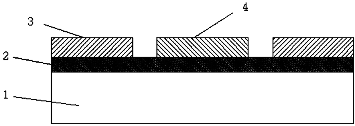
[0024] Such as figure 1 As shown, a gallium nitride Schottky barrier diode provided by the present invention includes a substrate and an epitaxial layer grown on the substrate, and an ohmic electrode and a Schottky electrode are arranged on the epitaxial layer. The Schottky electrode in this example can be circular or any other shape.

[0025] The substrate adopted in the present invention is a sapphire matrix, the epitaxial layer is an n-GaN layer, and the ohmic electrode on the epitaxial layer is a multilayer metal, which is successively titanium / aluminum / titanium / gold from bottom to top, and the titanium layer and The epitaxial layer is contacted, and the ohmic electrode is located at the periphery of the Schottky electrode.

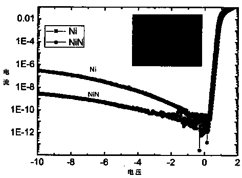
[0026] Wherein, the Schottky electrode includes a nickel nitride thin film layer, and the present invention replaces the nickel metal with the nickel nitride thin film layer as the Schottky contact, which can improve stability and reduce leakage curr...

Embodiment 2

[0037] A Gallium Nitride Schottky barrier diode provided by the present invention includes a substrate and an epitaxial layer grown on the substrate, and an ohmic electrode and a Schottky electrode are arranged on the epitaxial layer. In this embodiment, The Schottky electrode can be circular or any other shape.

[0038] Wherein, the Schottky electrode includes a nickel nitride thin film layer, and the present invention replaces the nickel metal with the nickel nitride thin film layer as the Schottky contact, which can improve stability and reduce leakage current.

[0039] Wherein, the epitaxial layer is an n-GaN layer.

[0040] The present invention also provides a method for manufacturing a Gallium Nitride Schottky barrier diode, comprising the following steps:

[0041] S1: The epitaxial layer of n-GaN is formed on the surface of the substrate by metal organic chemical vapor deposition;

[0042] S2: Use the magnetron sputtering method to sequentially form titanium / aluminum...

Embodiment 3

[0048] A Gallium Nitride Schottky barrier diode provided by the present invention includes a substrate and an epitaxial layer grown on the substrate, and an ohmic electrode and a Schottky electrode are arranged on the epitaxial layer. In this embodiment, The Schottky electrode can be circular or any other shape.

[0049]Wherein, the Schottky electrode includes a nickel nitride thin film layer, and the present invention replaces the nickel metal with the nickel nitride thin film layer as the Schottky contact, which can improve stability and reduce leakage current.

[0050] Wherein, the epitaxial layer is an n-GaN layer.

[0051] The present invention also provides a method for manufacturing a Gallium Nitride Schottky barrier diode, comprising the following steps:

[0052] S1: The epitaxial layer of n-GaN is formed on the surface of the substrate by metal organic chemical vapor deposition;

[0053] S2: Use the magnetron sputtering method to sequentially form titanium / aluminum / ...


PUM


Abstract

The invention discloses a gallium nitride Schottky barrier diode and a manufacturing method thereof. The gallium nitride Schottky barrier diode comprises a substrate and an epitaxial layer grown on the substrate, wherein the epitaxial layer is provided with an ohmic electrode and a Schottky electrode. The invention further discloses the manufacturing method of the gallium nitride Schottky barrierdiode. The manufacturing method comprises the steps of forming a nickel nitride thin film layer on a Schottky electrode region on the epitaxial layer by adopting a reactive magnetron sputtering methodin a nitrogen and argon atmosphere, then adopting a delamination method to form a Schottky contact and further form the Schottky electrode, and replacing nickel metal with the nickel nitride thin film layer to serve as a Schottky contact. The gallium nitride Schottky barrier diode and the manufacturing method thereof solve the technical problem that the diode stability is not good enough and thereverse leakage current is high in the prior art.

Description

technical field [0001] The invention relates to the technical field of semiconductors, in particular to a gallium nitride Schottky barrier diode and a manufacturing method thereof. Background technique [0002] Schottky barrier diodes (SBDs) are key devices in antenna rectifier (rectenna) circuits, and are widely used in microwave wireless power transmission systems, including electric vehicle power charging, energy harvesting, ubiquitous power supplies, and buildings. Wireless power distribution. However, traditional GaAs and Si-based commercial Schottky barrier diodes cannot meet the high conversion efficiency requirements of microwave wireless transmission technology at high frequency and high voltage. GaN-based materials have the characteristics of large band gap, high breakdown field, high electron mobility, and high electron saturation velocity. Therefore, GaN-based SBDs have received extensive attention in improving the efficiency of microwave wireless power transmis...

Claims


Application Information

Patent Timeline
Patent Type & Authority Applications(China)
IPC IPC(8): H01L29/47H01L29/872H01L21/329H01L21/285
CPCH01L21/28581H01L29/475H01L29/66143H01L29/872
Inventor 敖金平李小波邵春林林岳明
Owner 江西誉鸿锦芯片科技有限公司
Why Eureka
Try Eureka