Method for growing epitaxial structure of LED
A growth method and epitaxial structure technology, applied in electrical components, circuits, semiconductor devices, etc., can solve the problems of low quantum well radiation recombination efficiency, electron leakage, insufficient hole injection, etc., to suppress electron leakage, reduce stress, and effectively The effect of increasing the barrier height
- Summary
- Abstract
- Description
- Claims
- Application Information
AI Technical Summary
Problems solved by technology
Method used
Image
Examples
Embodiment 1
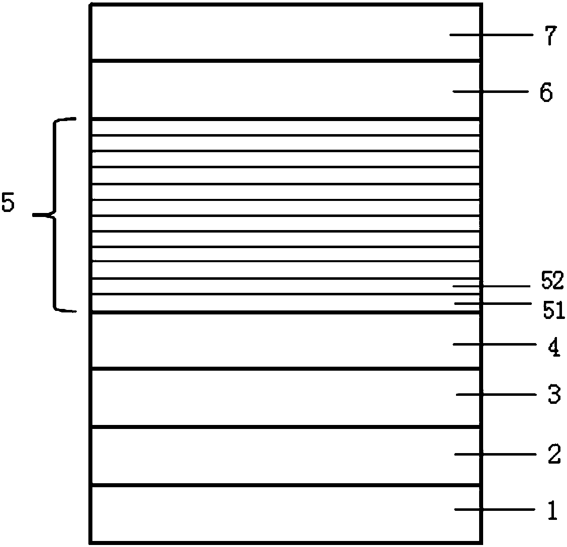
[0038] This embodiment adopts the LED epitaxial structure growth method provided by the present invention, adopts MOCVD to grow high-brightness GaN-based LED epitaxial wafers, and uses high-purity H 2 or high purity N 2 or high purity H 2 and high purity N 2 The mixed gas as the carrier gas, high-purity NH 3 As the N source, the metal-organic source trimethylgallium (TMGa) is used as the gallium source, trimethylindium (TMIn) is used as the indium source, and the N-type dopant is silane (SiH 4 ), trimethylaluminum (TMAl) as the aluminum source, and the P-type dopant as magnesium dicene (CP 2 Mg), the reaction pressure is between 70mbar and 900mbar. The specific growth method is as follows (for the epitaxial structure, please refer to figure 1 ):
[0039] A method for growing an LED epitaxial structure, which sequentially includes: processing a substrate, growing a low-temperature buffer layer GaN, growing an undoped GaN layer, growing an N-type GaN layer doped with Si, a...
PUM
 Abstract
Description
Claims
Application Information

