Preparation method of inclined table and preparation method of detector

A detector and mesa technology, applied in semiconductor devices, electrical components, circuits, etc., can solve problems such as jagged side walls and increased leakage current on the device surface

Active Publication Date: 2020-07-07
THE 13TH RES INST OF CHINA ELECTRONICS TECH GRP CORP
View PDF6 Cites 0 Cited by
  • Summary
  • Abstract
  • Description
  • Claims
  • Application Information

AI Technical Summary

Problems solved by technology

[0004] In view of this, an embodiment of the present invention provides a method for preparing an inclined mesa and a method for preparing a detector, so as to solve the problem that the inclination angle mesa prepared in the prior art has a jagged side wall, which leads to an increase in the leakage current on the surface of the device. question

Method used


Image

  • Preparation method of inclined table and preparation method of detector
  • Preparation method of inclined table and preparation method of detector
  • Preparation method of inclined table and preparation method of detector

Examples


preparation example Construction

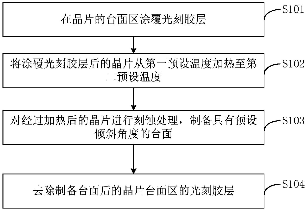
[0034] Please refer to figure 1 , the preparation method of inclined table comprises:

[0035] Step S101, coating a photoresist layer on the mesa region of the wafer.

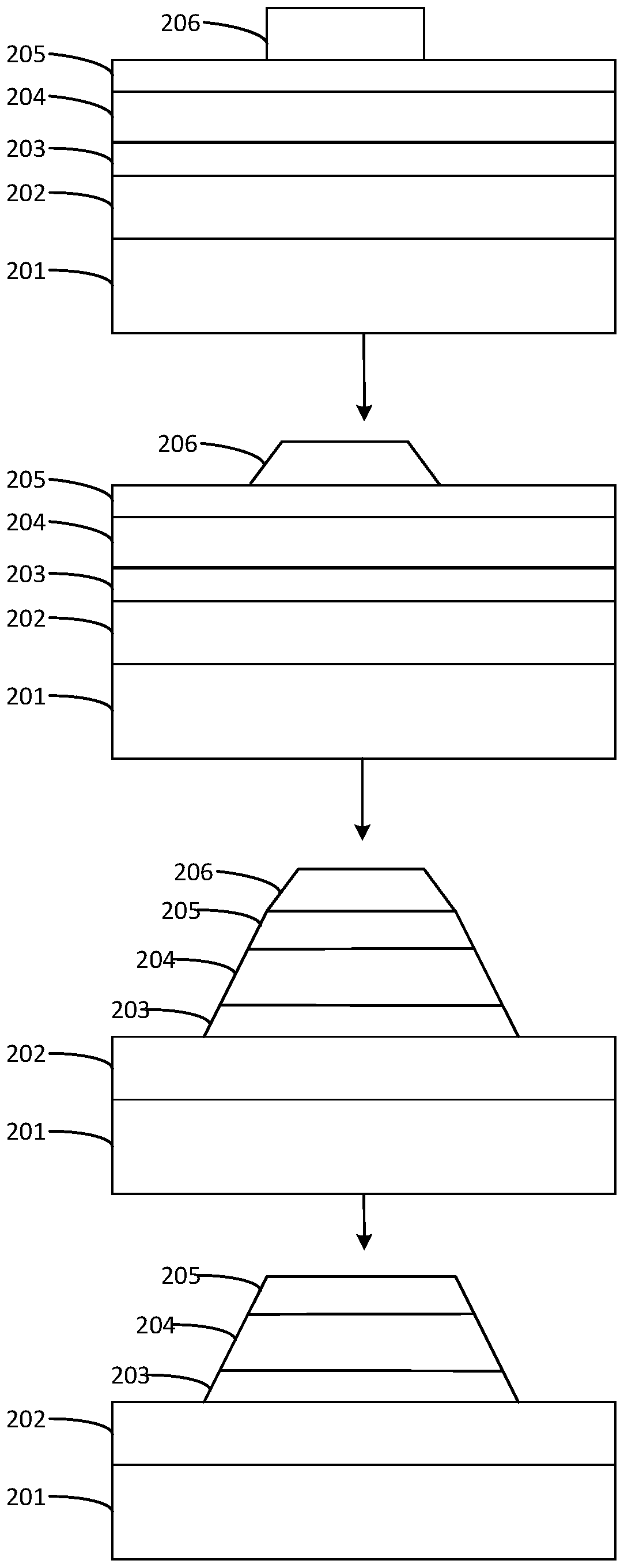
[0036] In the embodiment of the present invention, the wafer is a silicon carbide wafer, a gallium nitride wafer or other wafers capable of producing avalanche photodiodes. Preferably, the wafer is a silicon carbide wafer. Silicon carbide material is the preferred material for the preparation of ultraviolet photodetection devices due to its advantages such as large band gap, good thermal conductivity, high electron saturation drift velocity, stable chemical properties and low defect density. The mesa area of ​​the wafer is the area where the prepared mesa is located, please refer to figure 2 , coating a photoresist layer 206 on the mesa region of the wafer by spin coating.

[0037] Optionally, the wafer from bottom to top is substrate, silicon carbide P + layer, SiC N layer, SiC N - layer and SiC N + la...

Embodiment 2

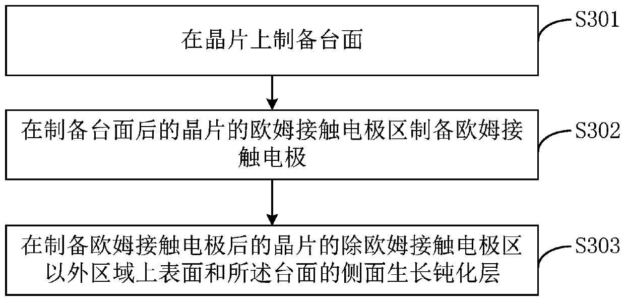
[0051] Please refer to image 3 , the preparation method of detector, comprising:

[0052] In step S301, a mesa is prepared on the wafer by the method described in Embodiment 1 of the present invention.

[0053] In the embodiment of the present invention, please refer to figure 2 , a mesa with a preset inclination angle and smooth sidewalls is prepared on the wafer by the method described in Embodiment 1 of the present invention.

[0054] Step S302 , preparing an ohmic contact electrode in the ohmic contact electrode area of ​​the wafer after the mesa is prepared.

[0055] In the embodiment of the present invention, please refer to Figure 4 , the ohmic contact electrode 207 is located on the upper surface of the mesa and the upper surface of the non-mesa area, wherein the non-mesa area is the area of ​​the wafer other than the mesa area. The ohmic contact electrode 207 on the upper surface of the mesa is an N-type electrode, the ohmic contact electrode 207 on the upper s...


PUM

PropertyMeasurementUnit
thicknessaaaaaaaaaa

Abstract

The present invention is applicable to the technical field of semiconductors, and provides a preparation method of an inclined mesa and a preparation method of a detector. The preparation method of an inclined mesa comprises: coating a photoresist layer on the mesa area of ​​a wafer, coating the photoresist layer The finished wafer is heated from the first preset temperature to the second preset temperature, and the heated wafer is etched to prepare a mesa with a preset inclination angle, and remove the photoresist layer in the mesa area of ​​the wafer after the mesa is prepared . The invention can make the side wall of the mesa very smooth, thereby reducing the leakage current on the surface of the device.

Description

technical field [0001] The invention belongs to the technical field of semiconductors, and in particular relates to a method for preparing an inclined table and a method for preparing a detector. Background technique [0002] Due to the absorption and scattering of ozone and other molecules in the atmosphere, ultraviolet radiation with a wavelength in the range of 100 nanometers to 280 nanometers hardly exists on the ground. With the advantages of small background interference and low false warning rate, it has important application prospects in the fields of ultraviolet early warning, ultraviolet communication, ultraviolet astronomy and other fields. [0003] A UV detector with a positively inclined mesa can effectively suppress the premature breakdown of the device, and the smaller the inclination angle of the mesa is, the better it is to suppress the premature breakdown of the device. Usually, the positive-tilt mesa is prepared by photoresist reflow method. At present, ...

Claims


Application Information

Patent Timeline
Patent Type & Authority Patents(China)
IPC IPC(8): H01L31/101H01L31/0236H01L31/18
CPCH01L31/0236H01L31/101H01L31/18H01L31/1812H01L31/107H01L31/02161H01L31/035281H01L31/022408H01L31/0312
Inventor 周幸叶冯志红吕元杰谭鑫王元刚宋旭波李佳房玉龙
Owner THE 13TH RES INST OF CHINA ELECTRONICS TECH GRP CORP
Why Eureka
Try Eureka