Total-reflection optical waveguide semiconductor laser chip and manufacturing method thereof

A laser and semiconductor technology, applied to the structure of optical waveguide semiconductors, etc., can solve problems affecting chip heat dissipation and increasing chip thermal resistance, and achieve the effects of eliminating stray light, improving reliability, and improving photoelectric conversion efficiency

Inactive Publication Date: 2018-10-09
Shandong Huaguang Optoelectronics Co. Ltd.
View PDF5 Cites 8 Cited by
  • Summary
  • Abstract
  • Description
  • Claims
  • Application Information

AI Technical Summary

Problems solved by technology

In this method, the upper surface of the contact layer except the top surface of the ridge is covered with a dielectric layer, which increases the thermal resistance of the chip and affects the heat dissipation of the chip.

Method used


Image

  • Total-reflection optical waveguide semiconductor laser chip and manufacturing method thereof
  • Total-reflection optical waveguide semiconductor laser chip and manufacturing method thereof
  • Total-reflection optical waveguide semiconductor laser chip and manufacturing method thereof

Examples


Embodiment 1

[0040] In this embodiment, taking a laser with a wavelength of 650 nm as an example, the preparation process of the semiconductor laser chip of the present invention is described in detail, which specifically includes the following steps.

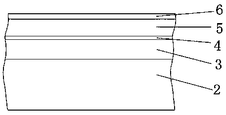
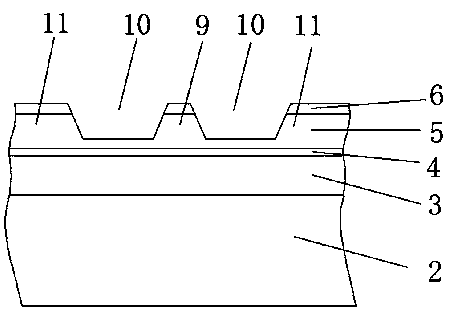
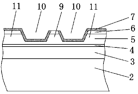
[0041] (1) Utilize the metal organic chemical vapor deposition method to grow the lower cladding layer 3, the active region 4, the upper cladding layer 5 and the ohmic contact layer 6 sequentially on the substrate 2 to form an epitaxial wafer, such as figure 1 shown.

[0042] (2) One-time photolithography: evenly cover a layer of photoresist on the ohmic contact layer 6, and form a ridge-shaped optical cavity 9 with a certain width according to the design requirements along the direction perpendicular to the cleavage of the epitaxial wafer through exposure, development and corrosion. The laser bar with a certain period and a certain width of the isolation groove 10, the height of the ridge optical cavity 9 is less than the thickness of the ...

Embodiment 808

[0057] In this embodiment, an 808nm wavelength laser is taken as an example.

[0058] The difference between this embodiment and embodiment 1 is:

[0059] In step (2), through exposure, development, and etching, along the direction perpendicular to the cleavage of the epitaxial wafer, a laser stripe structure with an optical cavity width of 50 microns, a period of 200 microns, and an isolation groove width of 20-30 microns is formed.

[0060] In step (3), each layer of SiO 2 Dielectric film thickness = 808nm*1 / (4*1.54) = 131nm, each layer of TiO 2 Dielectric film thickness=808nm*1 / (4*2.70)=75nm.


PUM


Abstract

A total-reflection optical waveguide semiconductor laser chip and a manufacturing method thereof are disclosed. The semiconductor laser chip comprises an epitaxial wafer. The epitaxial wafer comprisesa substrate, a lower cladding, an active area, an upper cladding and an Ohmic contact layer which are successively arranged from bottom to top. The center position of the epitaxial wafer is providedwith a ridge-type optical cavity. The two sides of the ridge-type optical cavity are provided with isolation grooves. The outer side of each isolation groove is provided with a shoulder area. The upper surface of the epitaxial wafer is provided with a high-reflectivity optical film layer and a P electrode layer. The manufacturing method comprises the following steps of (1) forming the epitaxial wafer; (2) carrying out one-time photoetching; (3) evaporating a high-reflectivity optical film; (4) carrying out two times of photoetching; (5) carrying out three times of photoetching; (6) manufacturing the P electrode layer; (7) carrying out substrate thinning; (8) manufacturing an N electrode layer; (9) carrying out strip dissociation and coating; and (10) forming a single laser chip. In the invention, the optical limiting of an optical cavity is realized, the threshold current of the laser chip is reduced, photoelectric conversion efficiency is increased, an output light shape is obviouslyimproved, stray light is eliminated and chip reliability is increased.

Description

technical field [0001] The invention relates to a total reflection optical waveguide semiconductor laser chip and a preparation method thereof, belonging to the technical field of semiconductor lasers. Background technique [0002] Semiconductor lasers have the advantages of small size, long life, low cost and high photoelectric conversion efficiency, and are widely used in industrial processing, lighting, communication, medical treatment and other fields. For semiconductor lasers, an important indicator is the light shape of the output light. There are many factors that affect the light shape, mainly the shape of the optical cavity, the refractive index of the medium layer on the side of the optical waveguide, etc. A qualified laser requires a clear outline of the main spot, no branching of the spot, and no stray spots. The output light shape of the laser depends on the light shape quality of the chip. There are two existing similar laser chip preparation processes. One i...

Claims


Application Information

Patent Timeline
Patent Type & Authority Applications(China)
IPC IPC(8): H01S5/22
Inventor 任忠祥苏建夏伟徐现刚
Owner Shandong Huaguang Optoelectronics Co. Ltd.
Why Eureka
Try Eureka