

Large-current low-forward-voltage-drop silicon carbide Schottly diode chip and preparation method thereof
A Schottky diode, voltage drop silicon carbide technology, applied in circuits, electrical components, semiconductor/solid-state device manufacturing, etc., can solve the problems of increasing device cost, increasing leakage current, and improving, and achieves lower device yield, The effect of increasing the manufacturing cost and overcoming the layout area
- Summary
- Abstract
- Description
- Claims
- Application Information
AI Technical Summary
Problems solved by technology
Method used
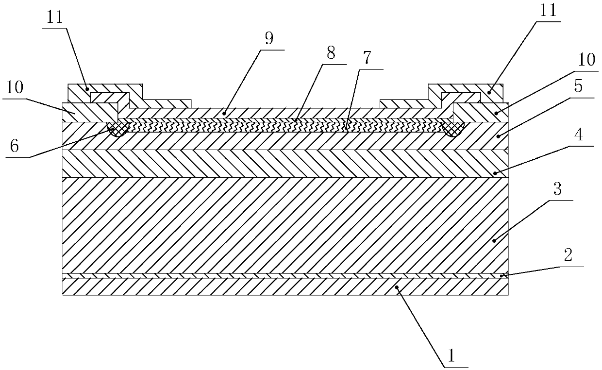
Image

Examples
Embodiment Construction
[0043]In order to make the purpose, technical solutions and advantages of the embodiments of the present invention clearer, the technical solutions in the embodiments of the present invention will be clearly and completely described below in conjunction with the drawings in the embodiments of the present invention. Obviously, the described embodiments It is a part of embodiments of the present invention, but not all embodiments. Based on the embodiments of the present invention, all other embodiments obtained by persons of ordinary skill in the art without making creative efforts belong to the protection scope of the present invention.
[0044] In describing the present invention, it is to be understood that the terms "central", "axial", "radial", "longitudinal", "transverse", "length", "width", "upper", "lower" , "Front", "Back", "Left", "Right", "Top", "Bottom", "Inner", "Outer", "Clockwise", "Counterclockwise", "Vertical", "Horizontal ” and other indicated orientations or ...
PUM
| Property | Measurement | Unit |
|---|---|---|
| thickness | aaaaa | aaaaa |
| thickness | aaaaa | aaaaa |
| thickness | aaaaa | aaaaa |
Abstract
Description
Claims
Application Information