
High-performance silicon-based elliptical gate tunneling field effect transistor

A tunneling field effect, high-performance technology, applied in special data processing applications, instruments, calculations, etc., can solve problems such as leakage current rise

Active Publication Date: 2018-11-02
FUDAN UNIV
View PDF6 Cites 0 Cited by
  • Summary
  • Abstract
  • Description
  • Claims
  • Application Information

AI Technical Summary

Problems solved by technology

[0002] The semiconductor industry has developed according to "Moore's Law" so far, and the integration of semiconductor chips has reached an astonishing level. However, due to the decrease of the channel length, the leakage current will increase exponentially, resulting in the problem of power consumption becoming more and more serious.

Method used


Image

  • High-performance silicon-based elliptical gate tunneling field effect transistor
  • High-performance silicon-based elliptical gate tunneling field effect transistor
  • High-performance silicon-based elliptical gate tunneling field effect transistor

Examples


Embodiment Construction

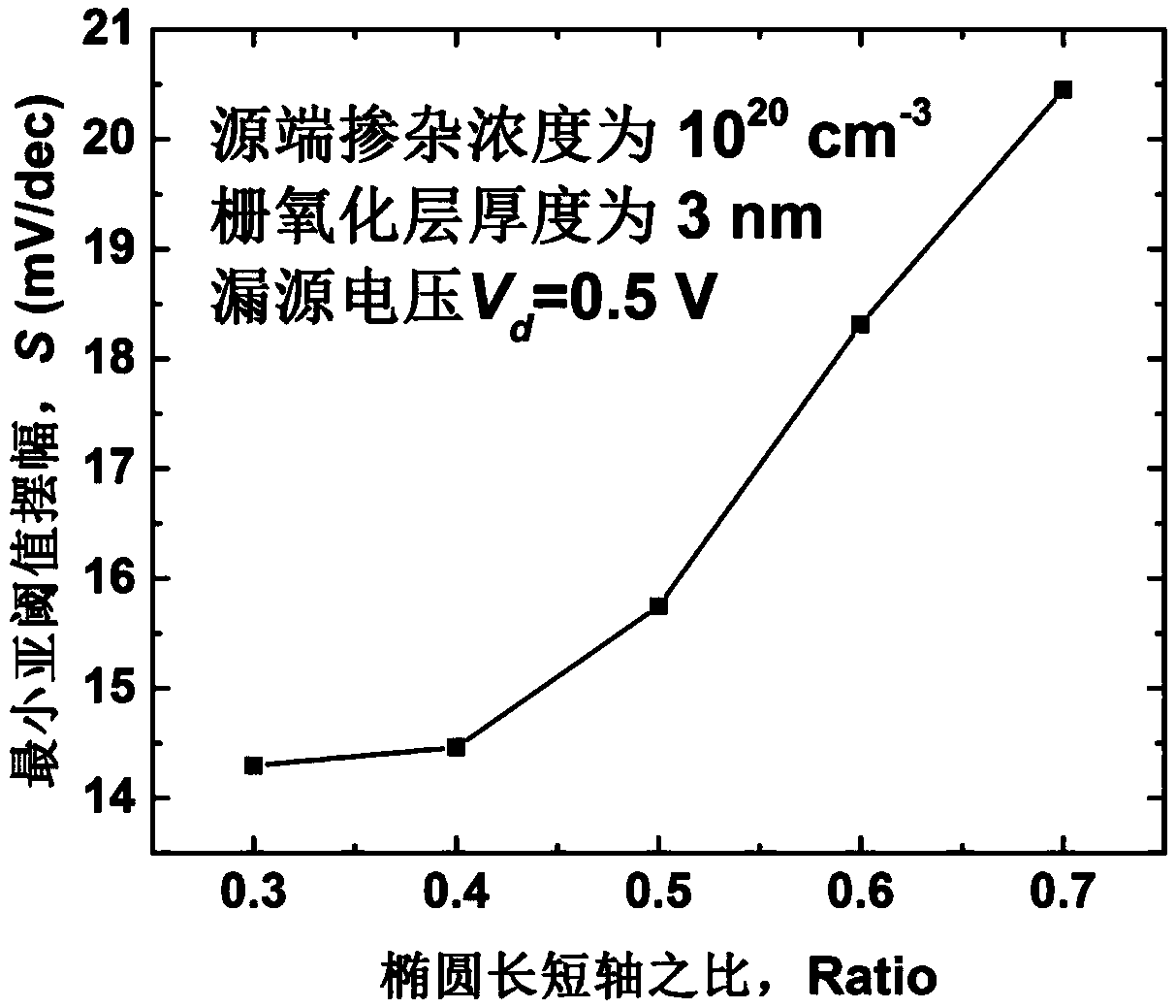
[0025] For the new silicon-based elliptical gate tunneling field effect transistor, we use Sentaurus 3D simulation software to simulate its electrical characteristics.

[0026] Use the Sentaurus Device Edit (SDE) component to create the corresponding structure. In the Sdvice component, the fluid dynamics model of the carrier transport equation, the Fermi Dirac distribution model, the forbidden band narrowing model, and the mobility model (including mobility and High electric field model and mobility and doping concentration model), carrier recombination model (including Shockley recombination, collision ionization correlation recombination and Auger recombination model), adding delocalized band-to-band tunneling model. After adding the above model to simulate, Figure 3 to Figure 8 for the simulation results.

[0027] In the simulated structure, the length of the channel is 40 nm, the length of the source and drain is 10 nm, and the thickness of the substrate oxide layer is ...


PUM

PropertyMeasurementUnit
Thicknessaaaaaaaaaa
Thicknessaaaaaaaaaa

Abstract

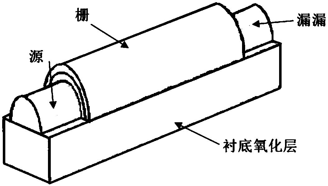
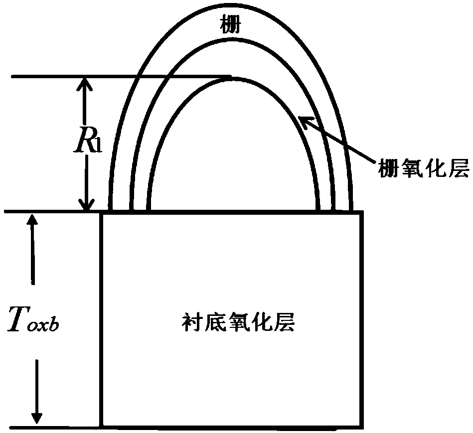
The invention belongs to the technical field of integrated circuit semiconductors, and particularly relates to a high-performance silicon-based elliptical gate tunneling field effect transistor. According to the structure, hafnium oxide is used as a substrate oxidation layer; semi-elliptic column type silicon serving as a channel and source-drain is arranged above the hafnium oxide; and an elliptic ring type hafnium oxide gate oxidation layer and a metal gate which have the same length-diameter ratio as the channel cover the channel. The p-type high-concentration boron doping is carried out onthe source end; the light n doping is carried out on the channel; and the n-type high-concentration phosphorus doping is carried out on the drain end. The field effect transistor takes transverse tunneling as a main tunneling mechanism, and can be regarded as a grid-controlled p-i-n junction. The simulation of simulation software shows that the tunneling field effect transistor has a good sub-threshold characteristic; the minimum sub-threshold swing can be as low as 20mV / dec and is smaller than the minimum sub-threshold swing, which is 60mV / dec, of a traditional MOSFET by three times; and a good design foundation is provided for practical development and application of tunneling devices.

Description

technical field [0001] The invention belongs to the technical field of integrated circuits and semiconductors, in particular to a high-performance silicon-based elliptical gate tunneling field effect transistor. Background technique [0002] The semiconductor industry has developed according to "Moore's Law" so far, and the integration of semiconductor chips has reached an astonishing level. However, due to the decrease of the channel length, the leakage current will increase exponentially, which will lead to the problem of power consumption becoming more and more serious. . In order to reduce power consumption, the most effective way at present is to reduce the power supply voltage when the device is working, and at the same time reduce the subthreshold leakage current and off-state current of the transistor. To this end, the concept of sub-threshold swing is introduced to represent the speed at which the device is turned on. The smaller S is, the faster the turn-on speed ...

Claims


Application Information

Patent Timeline
IPC IPC(8): G06F17/50
CPCG06F30/367
Inventor 胡光喜鲍佳睿胡淑彦刘冉郑立荣
Owner FUDAN UNIV
Learn More