Silicon carbide MOSFET device and manufacturing method thereof

A silicon carbide and device technology, applied in semiconductor/solid-state device manufacturing, semiconductor devices, electrical components, etc., can solve problems such as low work efficiency, high power loss, and poor robustness

Active Publication Date: 2018-11-13
HANGZHOU SILICON-MAGIC SEMICON TECH CO LTD
View PDF9 Cites 15 Cited by
  • Summary
  • Abstract
  • Description
  • Claims
  • Application Information

AI Technical Summary

Problems solved by technology

[0006] In view of the above problems, the present invention proposes a method that can optimize the poor robustness, high power loss, low work efficiency, and production cost of silicon carbide MOSFET devices in applications such as inverter circuits and chopper circuits due to excessive gate dielectric electric fields. Higher problem silicon carbide MOSFET device and method of manufacturing the same

Method used


Image

  • Silicon carbide MOSFET device and manufacturing method thereof
  • Silicon carbide MOSFET device and manufacturing method thereof
  • Silicon carbide MOSFET device and manufacturing method thereof

Examples


Embodiment 1

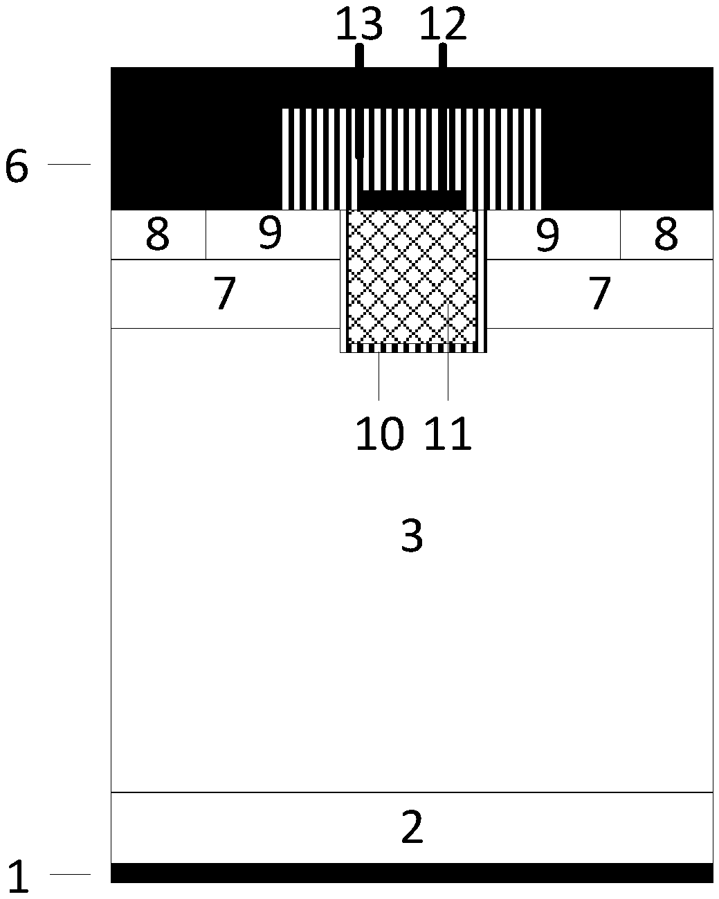
[0140] A silicon carbide MOSFET device, the cell structure of its basic structure is as follows figure 2 As shown, it includes metal drain 1, silicon carbide N + Substrate 2 and SiC N - epitaxial layer 3; the silicon carbide N - There is a first source trench on the upper left of the epitaxial layer 3, and there are silicon carbide P+ doped regions 5 and silicon carbide P-type doped regions 4 below the first source trench from top to bottom; the silicon carbide N - There is a second source trench on the upper right of the epitaxial layer 3, and there are silicon carbide P+ doped regions 5 and silicon carbide P-type doped regions 4 below the second source trench from top to bottom; both the first and second source trenches are filled Schottky contact metal 14 is formed; there is a gate trench above the silicon carbide N- epitaxial layer 3, the depth of which is shallower than the two source trenches, and a gate structure is formed inside and on the surface of the gate trench...

Embodiment 2

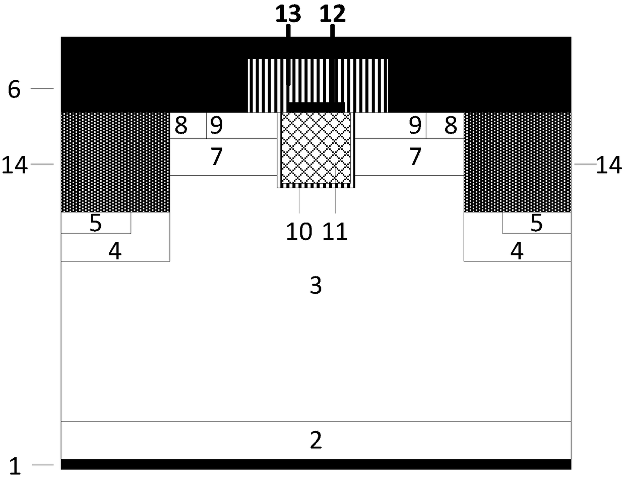
[0143] The structure of this embodiment is roughly the same as that of Embodiment 1, except that the Schottky contact metal 14 used is replaced by polysilicon 15, as image 3 shown. Also, a Si / SiC heterojunction structure with a rectifying contact is formed on the sidewall at the bottom of the source trench and the silicon carbide N-epitaxy 3 . The forward conduction voltage drop Von of the heterojunction structure is about 1.1V, which also has a greater effect on the operation of the third quadrant of the device. At the same time, since the heterojunction is a multi-sub-device, the diode has good reverse recovery performance.

Embodiment 3

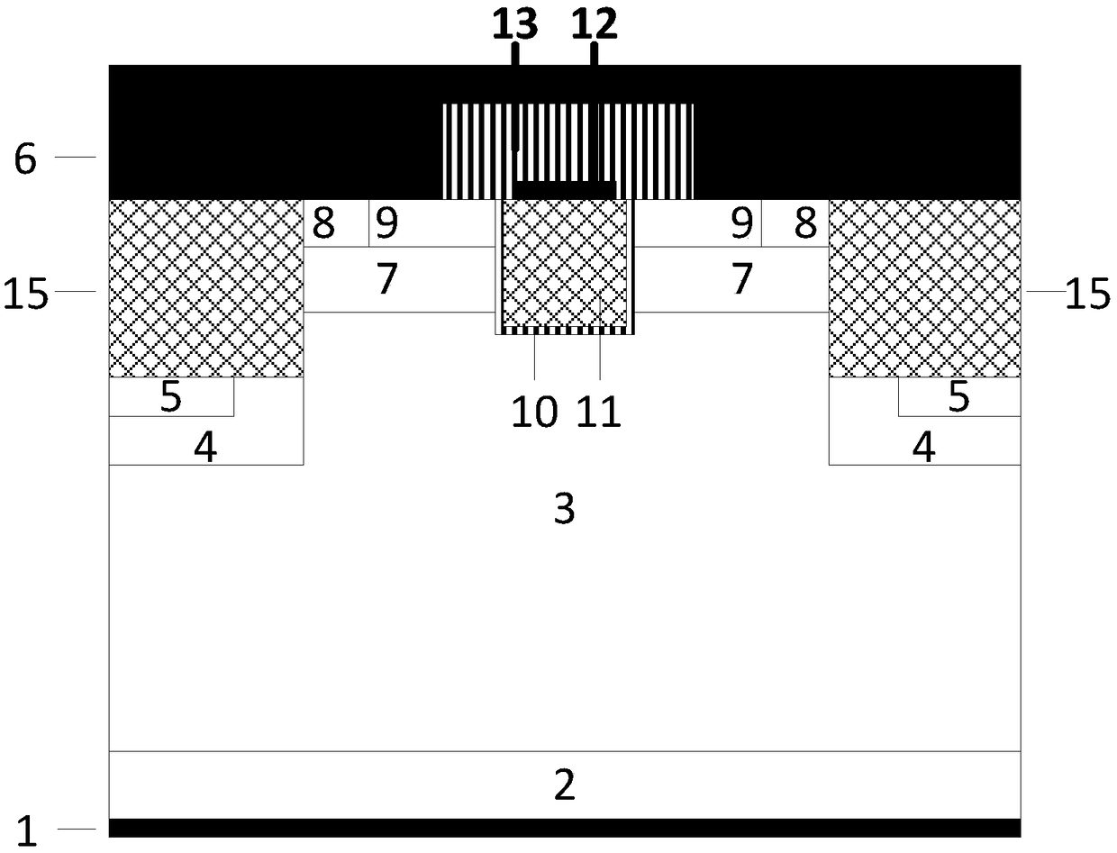
[0145] The difference between this embodiment and Embodiment 1 is that the bottom region of the gate structure has a split-gate structure, such as Figure 4shown. The split-gate structure includes a split-gate polysilicon 16 and a gate dielectric layer 10 surrounding the split-gate polysilicon 16 . The split-gate polysilicon 16 is led out by a metal lead at the back, which can be grounded or shorted to the source. This method significantly reduces the gate drain charge of the device, thereby reducing the Miller capacitance, and has a great optimization effect on improving the switching speed of the device.


PUM

PropertyMeasurementUnit
thicknessaaaaaaaaaa
widthaaaaaaaaaa
widthaaaaaaaaaa

Abstract

The invention provides a silicon carbide MOSFET device and a manufacturing method thereof. Silicon carbide deep P injection is performed in a specified region, groove etching and deposition of metal or polysilicon are performed above a silicon carbide deep P doped region, and the deposited metal or polysilicon is in direct contact with the silicon carbide N-epitaxy to form a Schottky contact or aSi/SiC heterojunction contact having rectifying characteristics. Therefore, the integration of multiple sub-rectifiers is achieve while optimizing the basic performance of the conventional silicon carbide UMOSFET, the working performance of the third quadrant of the device is greatly optimized, the gate-drain capacitance of the device is reduced and the switching speed of the device is improved.

Description

technical field [0001] The invention belongs to power semiconductor technology, in particular, relates to a metal oxide semiconductor field effect (MOSFET) device structure and a manufacturing method thereof. Background technique [0002] According to statistics, more than 90% of the electricity consumption in the world is controlled by power devices. Power devices and their modules provide an efficient way to realize the conversion of various forms of electric energy, and have been widely used in national defense construction, transportation, industrial production, medical and health and other fields. Since the first power device application in the 1950s, each generation of power devices has enabled more efficient conversion and use of energy. The history of power semiconductor devices, that is, the history of new power semiconductor devices. [0003] Traditional power devices and modules are dominated by silicon-based power devices, mainly thyristors, power PIN devices, ...

Claims


Application Information

Patent Timeline
Patent Type & Authority Applications(China)
IPC IPC(8): H01L29/06H01L29/16H01L21/336H01L29/78
CPCH01L29/0603H01L29/1608H01L29/66477H01L29/78
Inventor 张金平邹华罗君轶赵阳李泽宏张波
Owner HANGZHOU SILICON-MAGIC SEMICON TECH CO LTD
Why Eureka
Try Eureka