Silicon-based chip with mid-infrared spectrum signal enhancement function, and preparation method thereof

An infrared spectrum and signal technology, applied in the final product manufacturing, sustainable manufacturing/processing, antennas, etc., can solve the problems of compatibility of III-V semiconductors, unfavorable light modulation of nano-antenna sensors, and absorption of mid-infrared radiation. , to achieve the effect of improving stability and mass production

Active Publication Date: 2018-11-13
ZHEJIANG UNIV
View PDF2 Cites 8 Cited by
  • Summary
  • Abstract
  • Description
  • Claims
  • Application Information

AI Technical Summary

Problems solved by technology

However, this III-V semiconductor has dipole-activated optical phonons that absorb mid-infrared radiation, and if it is used to make molecular sensors, it is possible to cover the weak signals of the molecular spectrum
Moreover, this dipol

Method used


Image

  • Silicon-based chip with mid-infrared spectrum signal enhancement function, and preparation method thereof
  • Silicon-based chip with mid-infrared spectrum signal enhancement function, and preparation method thereof
  • Silicon-based chip with mid-infrared spectrum signal enhancement function, and preparation method thereof

Examples


Embodiment 1

[0062] A silicon-based chip with enhanced FTIR signal is fabricated as follows:

[0063] (1) Clean the silicon wafer with the standard RCA cleaning method. The specific steps of the RCA cleaning method are as follows:

[0064] (1-1) Ultrasonic cleaning with acetone solution for 5 to 20 minutes, and then repeated washing with deionized water to remove organic residues on the surface of the silicon wafer;

[0065] (1-2) Put the silicon wafer into an isopropanol solution and ultrasonically clean it for 5 to 20 minutes, and then rinse it repeatedly with deionized water to remove the acetone residue on the surface of the silicon wafer;

[0066] (1-3) Put the silicon chip into a mixed solution of ammonia, hydrogen peroxide and water (1:1:5 by volume) and boil for 10 to 20 minutes, then rinse it repeatedly with deionized water, and the particles attached to the surface of the silicon chip will is cleared in the mixed solution;

[0067] (1-4) Soak the silicon chip in 4% HF solution ...

Embodiment 2

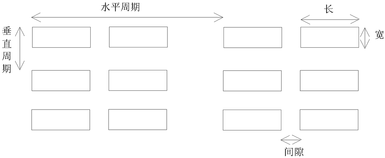
[0080] A silicon-based chip with enhanced FTIR signal function, the specific preparation process is the same as the process in Example 1, the difference is that the sub-wavelength microstructure array to be etched consists of a bow-tie antenna structure array (such as figure 2 shown) is transformed into a cuboid dipole antenna structure array (such as image 3 shown). A single dipole antenna structure consists of two cuboid structures facing each other in the long side direction. The cuboid has a length of 3 μm, a width of 0.8 μm, and a height of 1.5 μm. The period is 2 μm and the gap between the cuboids is 0.3 μm.

[0081] For the silicon-based chip with enhanced FTIR signal enhancement prepared in Example 2, the local plasmon resonance wavelength of the dipole antenna structure array is 9.4 μm, and the electric field strength near the hot spot of the electromagnetic field energy density is 31 times the initial incident electric field strength.

Embodiment 3

[0083] A silicon-based chip with enhanced FTIR signal function, the specific preparation process is the same as the process in Example 1, the difference is that the sub-wavelength microstructure array to be etched consists of a bow-tie antenna structure array (such as figure 2 shown) is transformed into a cylindrical structure array (such as Figure 4 shown). Each cylinder has a height of 1 μm, a diameter of 2 μm, and a period of 2.2 μm.

[0084] The silicon-based chip with enhanced FTIR signal enhancement prepared in embodiment 3, its electromagnetic field is respectively as follows Figure 5 As shown, the localized plasmon resonance wavelength of the cylindrical structure array is 8.0 μm, and the electric field strength near the hotspot of the electromagnetic field energy density is 13 times of the initial incident electric field strength.

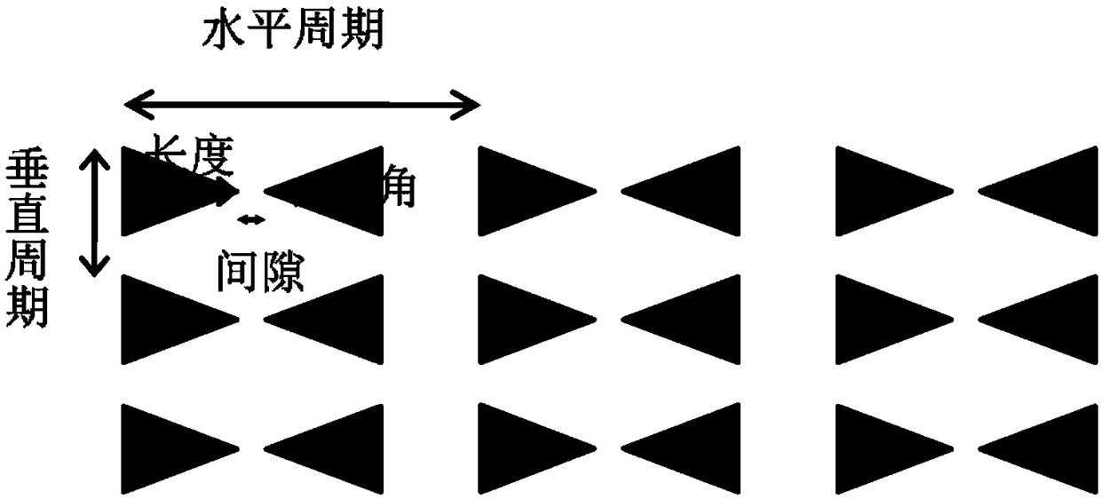
[0085] As can be seen from Examples 1 to 3, the water chestnut and the tip in the subwavelength microstructure array (bow-tie antenn...


PUM

PropertyMeasurementUnit
Growth temperatureaaaaaaaaaa
Thicknessaaaaaaaaaa

Abstract

The invention discloses a silicon-based chip with a mid-infrared spectrum signal enhancement function. The silicon-based chip comprises a silicon substrate, wherein the silicon substrate is sequentially provided with a Ge buffer layer and a heavily-doped Ge layer; and a sub-wavelength microstructure array is etched on the heavily-doped Ge layer. The invention further discloses a preparation methodof the silicon-based chip with the mid-infrared spectrum signal enhancement function. Compared with a III-V group semiconductor, the silicon-based chip with the mid-infrared spectrum signal enhancement function has weak lattice absorption characteristics, and is more suitable for being used as a molecular sensor chip material; and silicon is used as a substrate, so that the silicon-based chip canbe integrated with an electronic device in a monolithic integration mode conveniently, thereby highly improving stability and the yield of the device.

Description

technical field [0001] The invention relates to the field of silicon optoelectronics, in particular to a silicon-based chip capable of enhancing mid-infrared spectrum signals and a preparation method thereof. Background technique [0002] Fourier transform infrared spectroscopy (FTIR) has important applications in biomolecular detection, chemical harmful gas monitoring and other fields. Specifically, we can confirm the unique vibrational fingerprint region of the molecule (that is, the characteristic vibrational absorption peak of the molecule, which is generally located in the mid-infrared band with a wavelength range of 4-25 μm) by testing the infrared spectrum of the molecule, so as to identify the type of molecule and concentration. For example, in the field of medical detection, it has been found that the infrared spectra of normal tissues and cancerous tissues are significantly different, and the symmetrical stretching vibration peak (1080cm -1 ) was significantly hi...

Claims


Application Information

Patent Timeline
IPC IPC(8): H01L31/09H01L31/18H01Q1/22H01Q1/36
CPCH01L31/09H01L31/1804H01Q1/2283H01Q1/36Y02P70/50
Inventor 叶辉种海宁王哲玮徐泽民伍科
Owner ZHEJIANG UNIV
Why Eureka
Try Eureka