
Silica-based semiconductor-metal nano composite material and preparation method thereof

A technology of metal nano and composite materials, applied in the direction of nanotechnology, nanotechnology, nanotechnology for materials and surface science, etc., can solve the problems of inability to achieve full-spectrum absorption, insufficient heat conversion, and discounted photothermal effects. Achieve excellent light-to-heat conversion characteristics, broaden absorption spectrum, and high-efficiency structure

Active Publication Date: 2018-11-27
NANJING UNIV
View PDF7 Cites 12 Cited by
  • Summary
  • Abstract
  • Description
  • Claims
  • Application Information

AI Technical Summary

Problems solved by technology

The use of silicon nanopillars can improve the light absorption of silicon below 1100nm, but it has not been found that silicon nanowires sputtered with metals are used in photothermal reactions, because there are problems such as insufficient heat conversion, poor stability, short life, and the inability to achieve full-scale photothermal reactions. Spectrum absorption, photothermal effect is greatly reduced

Method used


Image

  • Silica-based semiconductor-metal nano composite material and preparation method thereof
  • Silica-based semiconductor-metal nano composite material and preparation method thereof
  • Silica-based semiconductor-metal nano composite material and preparation method thereof

Examples


Embodiment 1

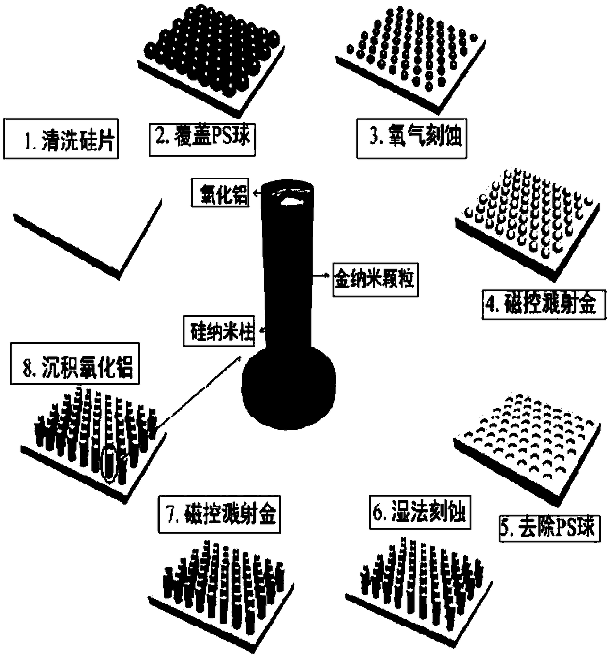
[0028] A silicon-based semiconductor-metal nanocomposite material provided in this embodiment has a structure such as figure 1 As shown: from the outside to the inside, it includes a high-temperature protection layer, a plasmon absorption layer, and an ordered silicon nanopillar array light-trapping layer; the high-temperature protection layer is aluminum oxide; the plasmon absorption layer is gold nanoparticles. The PS balls with a period of 1 μm used in this example, that is, the period of the silicon nanocolumn is 1 μm. Under this condition, the simulation calculation shows that when the diameter of the nanocolumn is about 400-600 nm, its antireflection performance is better, and at the same time, the nanocolumn The longer the length of the column, the better the anti-reflection performance, and the length of the prepared sample silicon nano-column is 1 μm to 3 μm.

[0029] Its preparation method is as follows:

[0030] 1) Clean the silicon wafer, clean the p-type single c...


PUM


Abstract

The invention relates to a silica-based semiconductor-metal nano composite material. The mateiral sequentially comprises a high-temperature protecting layer, a plasmon absorbing layer and an ordered silica nanorod array light trapping layer from outside to inside; the high-temperature protecting layer is aluminum oxide; the plasmon absorbing layer is gold nano particles. According to a periodic silica nano array structure with light trapping characteristics, light absorbing wavebands of silica can be broadened by spattering metal on the structure, the waveband is expanded from previously limited 1100 nm to full spectrum, photonic-like crystals are absorbed by optical resonant coupling of the periodic nano structure, and therefore the absorbing of the periodic nano structure is enhanced.

Description

technical field [0001] The invention relates to a silicon-based semiconductor-metal nanocomposite material and a preparation method thereof, belonging to the field of silicon-based photothermal conversion. Background technique [0002] Almost all substances in nature can exhibit the photothermal effect, that is, objects absorb photons of irradiated light and convert photon energy into heat energy. Among them, broadband and high-efficiency light absorption are prerequisites for high-efficiency light-to-heat conversion. Nano-metal particles with surface plasmon enhancement effect have unique light absorption characteristics. Individual nano-metal particles, such as gold, can only absorb light in a narrow band around its plasmon resonance peak. Nano-sized gold particles can achieve efficient broad-spectrum absorption, and high-efficiency broad-spectrum absorption has broad application prospects in solar cells and infrared imaging. At the same time, due to the existence of the...

Claims


Application Information

Patent Timeline
IPC IPC(8): F24S70/10B82Y30/00
CPCB82Y30/00
Inventor 徐骏侯国智吴仰晴宋小瑛刘剑刘婧婧
Owner NANJING UNIV
Learn More