Method for preparing a zinc oxide thin film transistor

A zinc oxide thin film, transistor technology, applied in transistors, semiconductor/solid-state device manufacturing, semiconductor devices and other directions, can solve the problems of poor electrical stability, low on-state current, etc., to improve on-state current, low cost, and potential application Effect

Active Publication Date: 2018-12-07
JILIN JIANZHU UNIVERSITY
View PDF5 Cites 2 Cited by
  • Summary
  • Abstract
  • Description
  • Claims
  • Application Information

AI Technical Summary

Problems solved by technology

[0004] The invention provides a method for preparing a zinc oxide thin film transistor to solve the existing problems of poor electrical stability and low on-state current

Method used


Image

  • Method for preparing a zinc oxide thin film transistor
  • Method for preparing a zinc oxide thin film transistor
  • Method for preparing a zinc oxide thin film transistor

Examples


Embodiment Construction

[0079] Include the following steps:

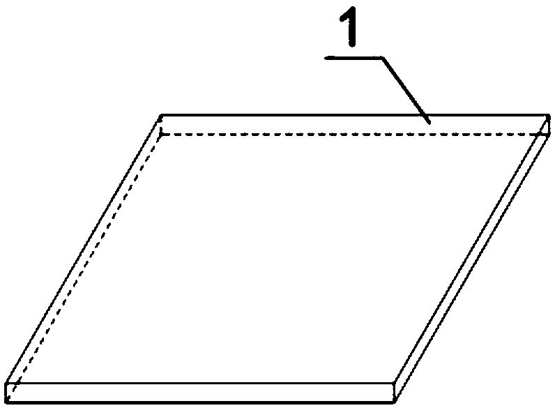
[0080] (1), clean the substrate 1, the substrate 1 adopts a hard substrate or a flexible substrate, and the substrate of this embodiment adopts glass; the specific steps are as follows:

[0081] (1) First put the substrate 1 into an acetone solution, and ultrasonically clean it at room temperature for 3 to 5 minutes to remove surface molecular contamination;

[0082] (2) Place the substrate 1 treated in step (1) in an ethanol solution, and ultrasonically clean it at room temperature for 3 to 5 minutes to remove residual acetone on the surface;

[0083] (3) Ultrasonic cleaning the substrate 1 treated in step (2) with deionized water at room temperature for 3 to 5 minutes to remove residual ethanol and ionic contamination;

[0084] (4) Dry the substrate 1 treated in step (3) with high-purity nitrogen, and put it in an oven for 5 minutes at 90°C, see figure 1 ;

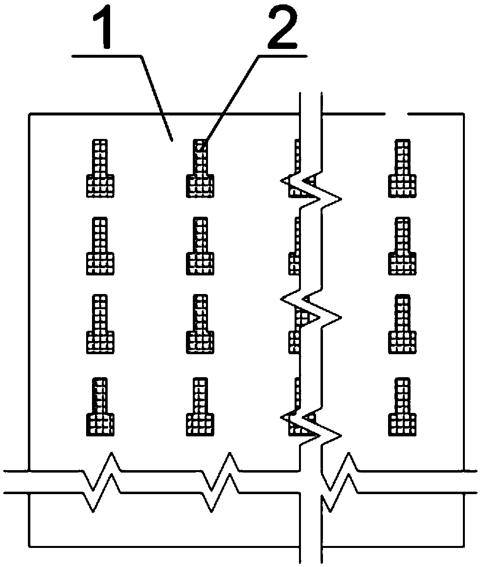
[0085] (2) Deposition of the gate 2, the gate material is a metal or oxide co...


PUM


Abstract

The invention relates to a method for preparing a zinc oxide thin film transistor, and belongs to a method for preparing a thin film transistor. The method includes substrate cleaning, gate deposition, insulating layer deposition, oxygen-rich zinc oxide channel layer deposition, low-oxygen zinc oxide channel layer deposition, and source electrode and drain electrode deposition. The method has theadvantages that through preparation of the double active layer structure and the interdigital source and drain electrodes, the oxygen-rich and low-oxygen layered channel layers are prepared to improvethe stability of the device and the on-state current, the source and drain electrodes of the interdigitated shape are prepared thereon to further greatly increases the on-state current, and the preparation process is simple. The method is commonly used in the market for RF magnetron sputtering and electron beam evaporation, and does not need to replace the production line; the raw material is pure zinc oxide, the cost is low, and environmental protection is achieved. The method has application prospects in the fields of ultraviolet detection and display driving. The pure zinc oxide thin filmtransistor has more potential application in the market.

Description

technical field [0001] The invention belongs to the technical field of semiconductor device preparation, and in particular relates to a preparation method of a thin film transistor. Background technique [0002] With the advent of the information age, the display field has entered the era of flat-panel display. As the core component of AMLCD and AMOLED, thin-film transistors have become an irreplaceable leading technology in the flat-panel display industry. The stability of thin-film transistors and various performance indicators The height of the display will directly limit the imaging capability of the display. Especially for large-size, high-resolution, high-frame-rate displays, such as three-dimensional displays, the requirements for the stability and driving force of thin-film transistors are more stringent, and the hydrogenated amorphous silicon thin-film transistors commonly used in the market can no longer meet the requirements. . In addition, since the driving mod...

Claims


Application Information

Patent Timeline
Patent Type & Authority Applications(China)
IPC IPC(8): H01L21/34H01L29/786H01L29/10H01L29/417
CPCH01L29/105H01L29/41733H01L29/66969H01L29/7869H01L29/78696
Inventor 高晓红张文通杨帆周路王欢赵阳闫兴振李彬吴博琦王超迟耀丹杨小天
Owner JILIN JIANZHU UNIVERSITY
Why Eureka
Try Eureka