Thin film transistor, display panel, and manufacturing method of thin film transistor

A technology for thin film transistors and glass substrates is applied in the production of display panels and thin film transistors.

Active Publication Date: 2018-12-11
深圳庸行科技有限公司
View PDF7 Cites 8 Cited by
  • Summary
  • Abstract
  • Description
  • Claims
  • Application Information

AI Technical Summary

Problems solved by technology

However, since metal oxides are extremely susceptible to the doping effect of impurities such as mobile metal ions, hydrogen ions, an

Method used


Image

  • Thin film transistor, display panel, and manufacturing method of thin film transistor
  • Thin film transistor, display panel, and manufacturing method of thin film transistor
  • Thin film transistor, display panel, and manufacturing method of thin film transistor

Examples


Embodiment Construction

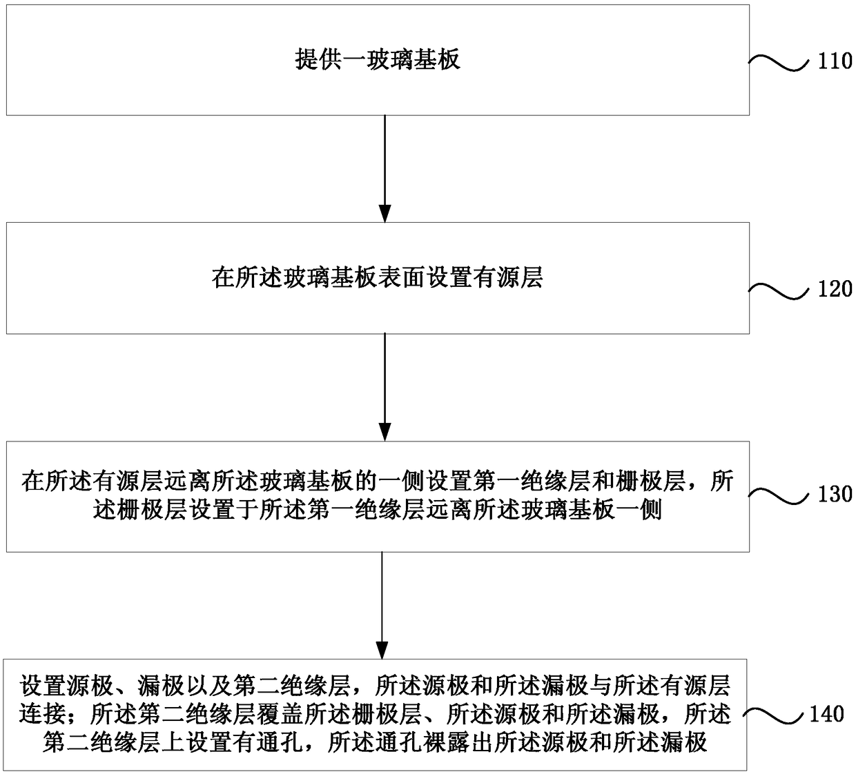
[0040] The present invention will be further described in detail below in conjunction with the accompanying drawings and embodiments. It should be understood that the specific embodiments described here are only used to explain the present invention, but not to limit the present invention. In addition, it should be noted that, for the convenience of description, only some structures related to the present invention are shown in the drawings but not all structures.

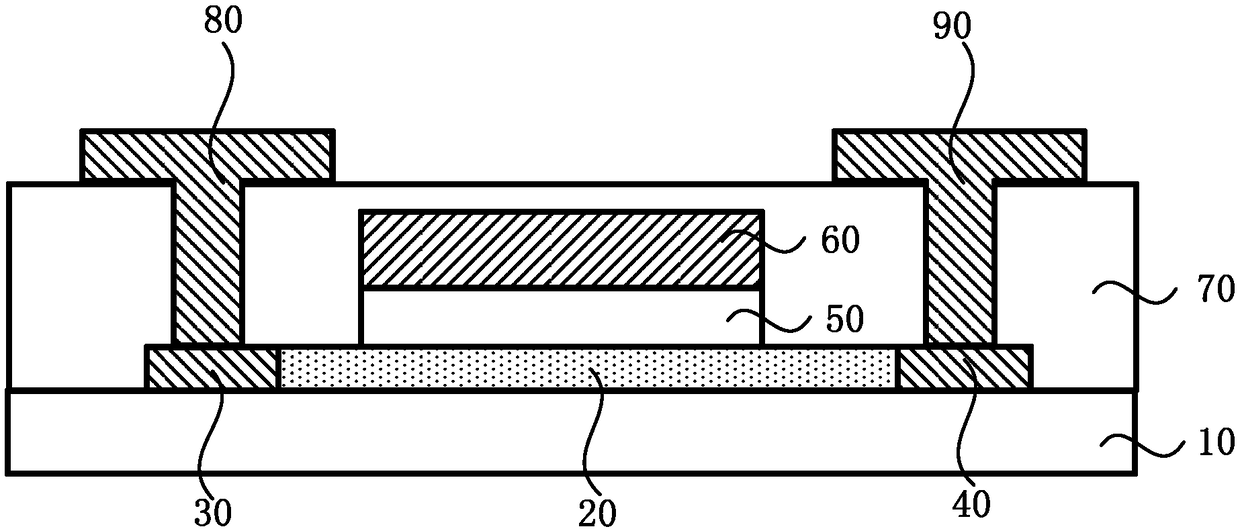
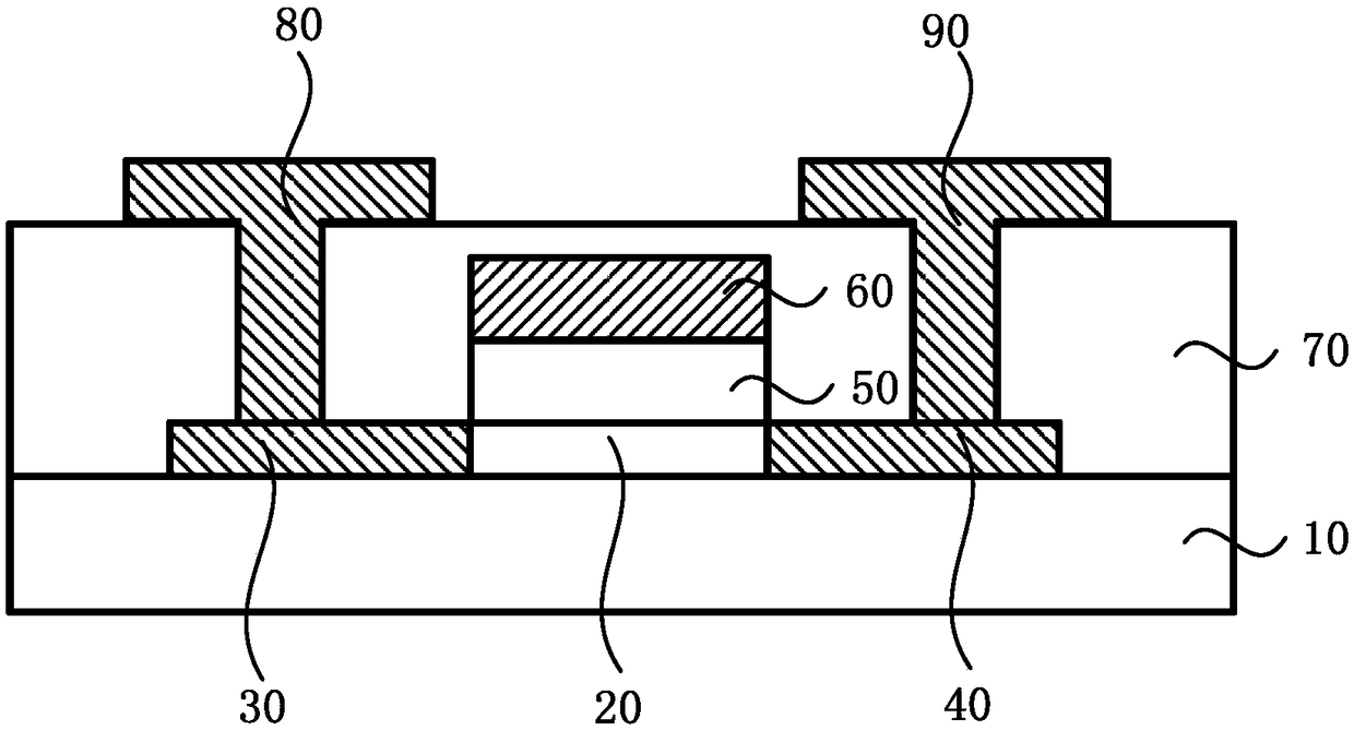
[0041] This embodiment provides a thin film transistor, figure 1 is a schematic structural diagram of a thin film transistor provided by an embodiment of the present invention, refer to figure 1 , the thin film transistor includes:

[0042] glass substrate 10;

[0043] The active layer 20, the source electrode 30 and the drain electrode 40, the active layer 20 is arranged on the surface of the glass substrate 10; the source electrode 30 and the drain electrode 40 are connected to the active layer 20;

[0044] T...


PUM


Abstract

The embodiment of the invention discloses a thin film transistor, a display panel and a manufacturing method of the thin film transistor. The thin film transistor comprises an active layer arranged onthe surface of a glass substrate, and a source electrode and a drain electrode are connected with the active layer. A first insulating layer disposed on a side of the active layer remote from the glass substrate; A gate layer disposed on a side of the first insulating layer remote from the glass substrate; The second insulating layer covers the source electrode, the drain electrode and the gate electrode layer, and the second insulating layer is provided with a through hole, and the through hole exposes the source electrode and the drain electrode; The active layer is made of (MO) x (RO) y (TO) z, where 0 (x (1, 0001 <=y <= 0. 20, 0.0001 <=z <= 0. 20, x+y+z=1; MO is a metal oxide, and M comprises at least one of In, Zn and Ga; RO is a rare earth oxide, and RO comprises at least one of praseodymium oxide, terbium oxide, dysprosium oxide and ytterbium oxide; TO is a transition metal oxide, and TO comprises at least one of vanadium oxide, niobium oxide and tantalum oxide. Embodiments ofthe present invention provide a low cost top gate structure metal oxide thin film transistor.

Description

technical field [0001] Embodiments of the present invention relate to semiconductor technology, and in particular, to thin film transistors, display panels, and manufacturing methods of thin film transistors. Background technique [0002] The core technology of the new flat panel display industry is thin film transistor (TFT, Thin Film Transistor) backplane technology. Metal oxide TFT (MO-TFT, Metal Oxide-TFT) not only has high mobility (at 1-100cm 2 / (V*s) or so), and the manufacturing process is relatively simple, compatible with the current a-Si process, the manufacturing cost is low, and it also has excellent large-area uniformity. Therefore, MO-TFT technology has attracted the attention of the industry since its birth. However, since metal oxides are extremely susceptible to the doping effect of impurities such as mobile metal ions, hydrogen ions, and oxygen vacancies, an etch barrier structure with channel protection is usually used, and it is difficult to use a top ...

Claims


Application Information

Patent Timeline
IPC IPC(8): H01L29/24H01L29/786H01L21/34
CPCH01L29/24H01L29/66969H01L29/78603H01L29/7869
Inventor 徐苗李民彭俊彪王磊陶洪邹建华
Owner 深圳庸行科技有限公司
Why Eureka
Try Eureka