A packaging method of a QFN fingerprint identification chip

A technology of fingerprint identification and packaging method, which is applied in the manufacturing of electrical components, electric solid-state devices, semiconductor/solid-state devices, etc., can solve the problems of difficult cutting of lead frames, decreased packaging yield, and easy to break, and solves the problem of easy breakage. , the effect of reducing shear deviation and increasing toughness

Inactive Publication Date: 2018-12-18
星科金朋半导体(江阴)有限公司
View PDF9 Cites 3 Cited by
  • Summary
  • Abstract
  • Description
  • Claims
  • Application Information

AI Technical Summary

Problems solved by technology

However, QFN products are ultra-thin products. The plastic cover becomes thinner and thinner after grinding, and the risk of fracture is extremely prone to occur; the thickness of the lead frame is also thinner and thinner, which makes the lead frame unable to bear Huge pulling and impact force, resulting in deformation, and then, during the cutting process of packaged products, the deformed lead frame makes cutting difficult
Even the huge amount of deformation causes the pins to still be connected, resulting in a short circuit of the product and a decrease in the packaging yield

Method used


Image

  • A packaging method of a QFN fingerprint identification chip
  • A packaging method of a QFN fingerprint identification chip
  • A packaging method of a QFN fingerprint identification chip

Examples


Embodiment

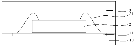
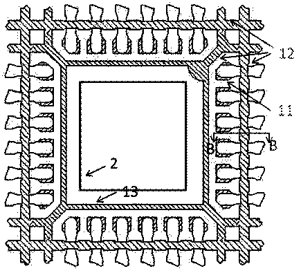
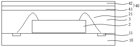
[0078] The packaging structure of the QFN fingerprint identification chip involved in the present invention, such as figure 2 As shown, the chip 2 is arranged in the middle area of ​​the lead frame 10 and fixedly connected with the lead frame 10 . Specifically, the lead frame 10 includes a chip holder, connecting ribs 12 and gold fingers 11, and is the carrier of the chip 2. The chip 2 is fixed on the chip holder, and the aluminum pad on the chip 2 is connected to the gold finger 11 in a one-to-one correspondence using a bonding wire 21. , the gold finger 11 on the remaining side is fixedly connected to the chip holder, and the chip 2 is electrically connected to the gold finger 11 to transmit the electrical signal to the structure of the external PCB board. The chip 2 is a silicon-based fingerprint chip, and in other embodiments, it may also be a chip of other materials or functions. The plastic package 3 wraps the front surface of the lead frame 10 , the chip 2 and the bon...


PUM


Abstract

The invention discloses a packaging method of a QFN fingerprint identification chip, belonging to the technical field of semiconductor chip packaging. The process comprises the following steps: mounting a loading film on the back of a lead frame; adhering the chip to the lead frame; curing silver paste; performing plasma cleaning; performing wire bonding; performing plastic packaging; removing theloading film; performing post curing; removing residual glue; baking; thinning a plastic cover and pasting a reinforcing film; cutting off a connecting rib to carry out a strip test; printing a marking; removing the reinforcing film; and cutting for molding. The invention provides a packaging method capable of improving the yield of QFN fingerprint identification chip packaging.

Description

technical field [0001] The invention relates to a packaging method of a QFN fingerprint recognition chip, in particular to a packaging method of a packaging structure of a QFN fingerprint recognition chip with a development trend of being large and thin, and belongs to the technical field of semiconductor chip packaging. Background technique [0002] Fingerprint identification technology is a systematic technical system, which involves a relatively complex industrial chain, involving fingerprint chip manufacturers, fingerprint identification module manufacturers, fingerprint identification solution providers, mobile phone terminal manufacturers, and software application vendors. From chip, package, coating, cover plate, metal ring, to the final module, all links have begun to work hard to break through the bottleneck. [0003] At present, Substrate packaging is generally used in the field of fingerprint recognition. The price of fingerprint modules keeps falling. As the pr...

Claims


Application Information

Patent Timeline
Patent Type & Authority Applications(China)
IPC IPC(8): H01L21/56H01L21/48
CPCH01L21/4821H01L21/56H01L2224/48091H01L2224/73265H01L2924/00014
Inventor 熊伟陶军峰李越付雷雷熊辉沈国强刘仁琦
Owner 星科金朋半导体(江阴)有限公司
Why Eureka
Try Eureka