A bonding pad for vertical interconnection with a ceramic circuit substrate BGA and a manufacturing method thereof

A technology for circuit substrates and ceramics, applied in circuits, electrical components, electrical solid devices, etc., can solve the problems of large shear stress, thermal expansion coefficient difference, reliability research and optimization are not in-depth, etc., to improve shear strength, increase Soldering area, the effect of high reliability BGA interconnection

Inactive Publication Date: 2018-12-18
SOUTHWEST CHINA RES INST OF ELECTRONICS EQUIP
View PDF10 Cites 1 Cited by
  • Summary
  • Abstract
  • Description
  • Claims
  • Application Information

AI Technical Summary

Problems solved by technology

[0004] Generally speaking, the BGA interconnection of ceramic circuit substrates has a broad application space in the field of high-frequency transmission, but at present it mainly focuses on the research of electrical transmission performance, and the reliability research and optimization are not deep, especiall

Method used


Image

  • A bonding pad for vertical interconnection with a ceramic circuit substrate BGA and a manufacturing method thereof
  • A bonding pad for vertical interconnection with a ceramic circuit substrate BGA and a manufacturing method thereof
  • A bonding pad for vertical interconnection with a ceramic circuit substrate BGA and a manufacturing method thereof

Examples


Embodiment

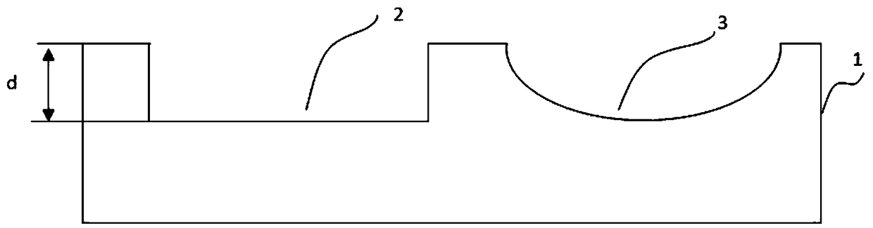
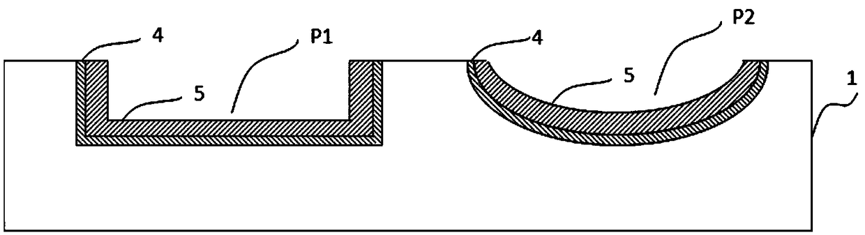
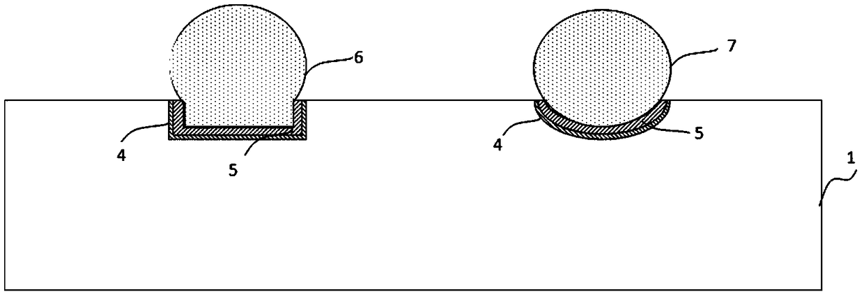
[0035] Such as figure 1 and figure 2 As shown, a pad for vertical interconnection of a ceramic circuit substrate BGA includes pits, a metallized seed layer 4 and a metallized film layer 5, the pits are arranged on the surface of the ceramic circuit substrate 1, and the pits The vertical section can be arc-shaped or polygonal, such as rectangular pit 2, arc-shaped pit 3, the metallized seed layer 4 is arranged on the surface of the pit, and the metallized film layer 5 is arranged on the surface of the pit. The surface of the seed layer 4 is metallized.

[0036] In the above technical solution, due to the design of the pit structure, the pads are concave downwards and have a three-dimensional structure, which can better clamp the solder balls and increase the soldering area, improve the shear strength of the solder balls, and achieve high reliability of the ceramic circuit board. BGA interconnection. The pad structure does not change the circuit layout and electrical transmi...

experiment example 1

[0052] Experimental Example 1 The influence of the three-dimensional structure pad of the present invention on the shear force of BGA balls

[0053] 1. BGA ball shear force test welded with three-dimensional structure pads of the present invention

[0054] 1) The LTCC substrate of Dupont's 9K7 system is used as the processing object, and the total thickness of the substrate is 1.5mm. A pit with a depth of d=17 μm is processed on the surface of the substrate by laser etching, and the diameter of the pit is 0.6 mm;

[0055] 2) Make a metallized seed layer on the pit by thin film sputtering process, the total thickness of the seed layer is 260nm, the composition is Ti thickness 75nm, W thickness 75nm, Au thickness 110nm;

[0056] 3) A metallization layer for tin-lead soldering is made on the seed layer by using an electroless plating process, and the components are a Ni layer with a thickness of 4 μm, a Pd layer with a thickness of 0.1 μm, and an Au layer with a thickness of 0.1...


PUM

PropertyMeasurementUnit
Long diameteraaaaaaaaaa
Depthaaaaaaaaaa
Thicknessaaaaaaaaaa

Abstract

The invention discloses a bonding pad for vertical interconnection with a ceramic circuit substrate BGA, comprising a pit, a metallization seed layer and a metallization film layer, wherein the pit isarranged on the surface of the ceramic circuit substrate, the metallization seed layer is arranged on the surface of the pit, and the metallization film layer is arranged on the surface of the metallization seed layer. A pad for vertical interconnection of a ceramic circuit board BGA is provided, As the bonding pad is concave downward and has a three-dimensional structure due to the design of thepit structure, the boning pad can be made on the surface of the ceramic circuit substrate, the solder ball can be clamped well, the solder area can be increased, the shear strength of the solder ballcan be improved, and the high-reliable BGA interconnection of the ceramic circuit substrate can be realized.

Description

technical field [0001] The invention relates to the technical field of manufacturing ceramic circuit substrates, in particular to a method for manufacturing solder pads for BGA vertical interconnection of ceramic circuit substrates. Background technique [0002] Ceramic circuit substrates typically represented by LTCC (low temperature co-fired ceramics) have outstanding advantages such as high integration density, microwave / digital / control multifunctional hybrid integration, and excellent high-frequency performance. field has been widely applied. With the continuous development of miniaturization and multi-function, broadband microwave components are gradually changing to the form of three-dimensional stacking of SIP modules. Therefore, the high-frequency, high-performance, and high-reliability vertical interconnection of ceramic circuit substrates has become a key factor restricting three-dimensional stacking of substrates. [0003] Commonly used vertical interconnection m...

Claims


Application Information

Patent Timeline
IPC IPC(8): H01L23/498H01L21/48
CPCH01L21/4846H01L23/49816H01L23/49838H01L23/49866H01L2224/11
Inventor 岳帅旗杨宇刘志辉张刚徐洋
Owner SOUTHWEST CHINA RES INST OF ELECTRONICS EQUIP
Why Eureka
Try Eureka