A flexible substrate and a preparation method thereof

A flexible substrate and film technology, applied in the direction of climate sustainability, final product manufacturing, sustainable manufacturing/processing, etc., can solve the problem of transistor device characteristic failure, flexible display device display quality degradation, and OLED device luminous efficiency. life and other issues, to achieve the effect of extending the service life

Inactive Publication Date: 2018-12-18
EVERDISPLAY OPTRONICS (SHANGHAI) CO LTD
View PDF11 Cites 14 Cited by
  • Summary
  • Abstract
  • Description
  • Claims
  • Application Information

AI Technical Summary

Problems solved by technology

[0005] Since the wavelength of the selected laser is generally 308-360nm, such laser light will pass through the flexible substrate and irradiate the thin film transistor and OLED module on the other side of the flexible substrate, which will not only cause the threshold voltage drift of the t

Method used


Image

  • A flexible substrate and a preparation method thereof

Examples


preparation example Construction

[0044] The preparation method of the flexible substrate of the present invention comprises the following steps:

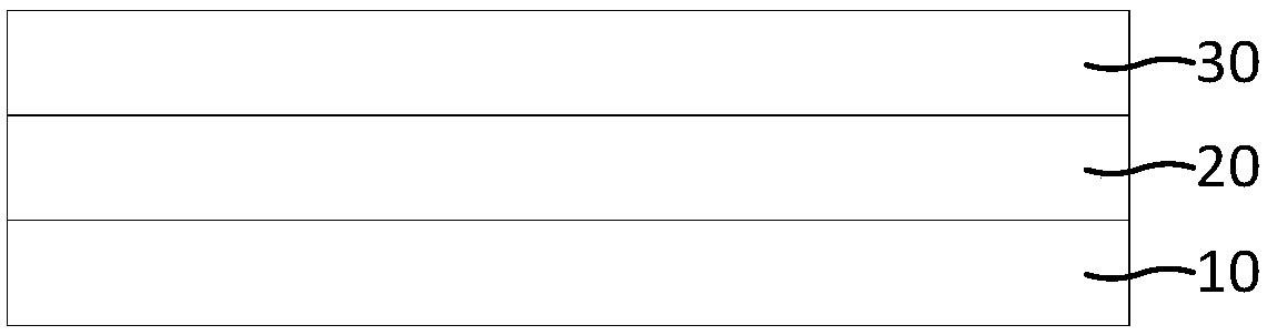
[0045] (1) Prepare an organic polymer precursor, add nanoparticles to the organic polymer precursor, the nanoparticles are selected from at least one substance in titanium oxide, zinc oxide or silicon oxide, and coat it on a hard substrate The organic polymer precursor doped with nanoparticles is heated and cured to obtain the first film layer 10 .

[0046] The hard substrate is used as a carrier to support the subsequent flexible substrate, thin film transistor and OLED module. After the flexible display device is prepared, it is separated from the flexible display device after laser lift-off. As an example, a glass substrate may be used as the hard substrate.

[0047] The organic polymer precursor, that is, the state in which the organic polymer exists before forming the organic polymer film, may be a solution composed of raw materials for the organic polymer, o...

Embodiment

[0056] (1) Prepare the first film layer 10 on the hard substrate.

[0057] Dissolve 4,4'-diaminodiphenyl ether in N,N-dimethylacetamide, and mechanically stir until 4,4'-diaminodiphenyl ether is completely dissolved to obtain a mixed solution; then add to the above mixed solution Add an equimolar amount of 3,3',4,4'-diphenyl ether tetracarboxylic dianhydride, stir mechanically until the 3,3',4,4'-diphenyl ether tetracarboxylic dianhydride is completely dissolved, and continue stirring for 2h~ After 4h, a polyamic acid (PAA) solution was obtained. Then adding nano-SiO to the polyamic acid (PAA) solution 2 , after stirring or ultrasonic dispersion, the nano-SiO 2 Uniformly dispersed in polyamic acid (PAA) solution to obtain the precursor of polyimide (PI) doped with nanoparticles.

[0058] Use a low-speed rotary film coater to coat one surface of a glass substrate, place it in a thermal oven or an IR furnace for heating and curing, and the heating temperature is 150 ° C to 30...


PUM

PropertyMeasurementUnit
Thicknessaaaaaaaaaa
Thicknessaaaaaaaaaa
Thicknessaaaaaaaaaa

Abstract

The invention provides a flexible substrate, comprising a first film layer, a second film layer and a third film layer which are laminated in sequence, wherein the first film layer and the third filmlayer are organic polymer films doped with nano particles selected from at least one substance of titanium oxide, zinc oxide or silicon oxide; and the second film layer is an inorganic film. The invention also provides a preparation method of the flexible substrate and a flexible display device including the flexible substrate. By doping nanoparticles in the first film layer and the third film layer of the flexible substrate, ultraviolet rays during laser peeling can be effectively absorbed or reflected, thereby preventing laser from causing damage to the thin film transistor and the OLED module on the other side of the flexible substrate.

Description

technical field [0001] The invention relates to the field of display technology, in particular to a flexible substrate and a method for preparing the flexible substrate. Background technique [0002] Organic electroluminescent devices (OLEDs) have the characteristics of low power consumption, light weight, high brightness, wide field of view and fast response, and can realize flexible displays. They have been applied to smart terminals such as smartphones and tablet computers, and gradually become a new generation of display product. [0003] Since flexible display devices have the advantages of rollability, impact resistance, strong shock resistance, light weight, small size, and more convenient portability, with the development of technology, they have been more and more widely used, and the application prospects are very promising. Obviously, the substrate used in the flexible display device must be a flexible substrate, such as polyimide (PI), polyethylene terephthalate...

Claims


Application Information

Patent Timeline
IPC IPC(8): H01L51/50H01L51/56H01L27/32
CPCH10K59/12H10K77/111H10K50/00H10K71/00Y02E10/549Y02P70/50
Inventor 张其国
Owner EVERDISPLAY OPTRONICS (SHANGHAI) CO LTD
Why Eureka
Try Eureka