A structure of SiC UMOSFET integrated with SBD and a preparation method thereof

A main trench, n-type technology, applied in semiconductor/solid-state device manufacturing, electrical components, electrical solid-state devices, etc. Problems such as the increase of the leakage current of the special base diode can achieve the effects of improving carrier mobility, good on-state characteristics, and reducing the number of packages and costs.

Inactive Publication Date: 2018-12-21
INST OF SEMICONDUCTORS - CHINESE ACAD OF SCI
View PDF3 Cites 10 Cited by
  • Summary
  • Abstract
  • Description
  • Claims
  • Application Information

AI Technical Summary

Problems solved by technology

However, the integration of SBD devices in SiC UMOSFET cells requires attention to the problem of excessive electric field in the trench oxide under the reverse blocking voltage, especially the two-dimensional electric field accumulation at the corner of the bottom trench; attention also needs to be paid to the position of the Schottky contact The problem of excessive electric field, especially the increase of Schottky diode leakage current caused by the image force under high temperature working conditions, is not conducive to the improvement of high temperature and high field reliability of integrated chips

Method used


Image

  • A structure of SiC UMOSFET integrated with SBD and a preparation method thereof
  • A structure of SiC UMOSFET integrated with SBD and a preparation method thereof
  • A structure of SiC UMOSFET integrated with SBD and a preparation method thereof

Examples


Embodiment Construction

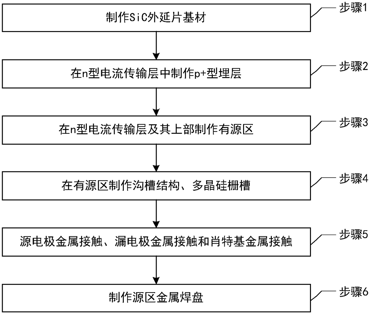
[0046] In order to make the object, technical solution and advantages of the present invention clearer, the present invention will be further described in detail below in conjunction with specific embodiments and with reference to the accompanying drawings.

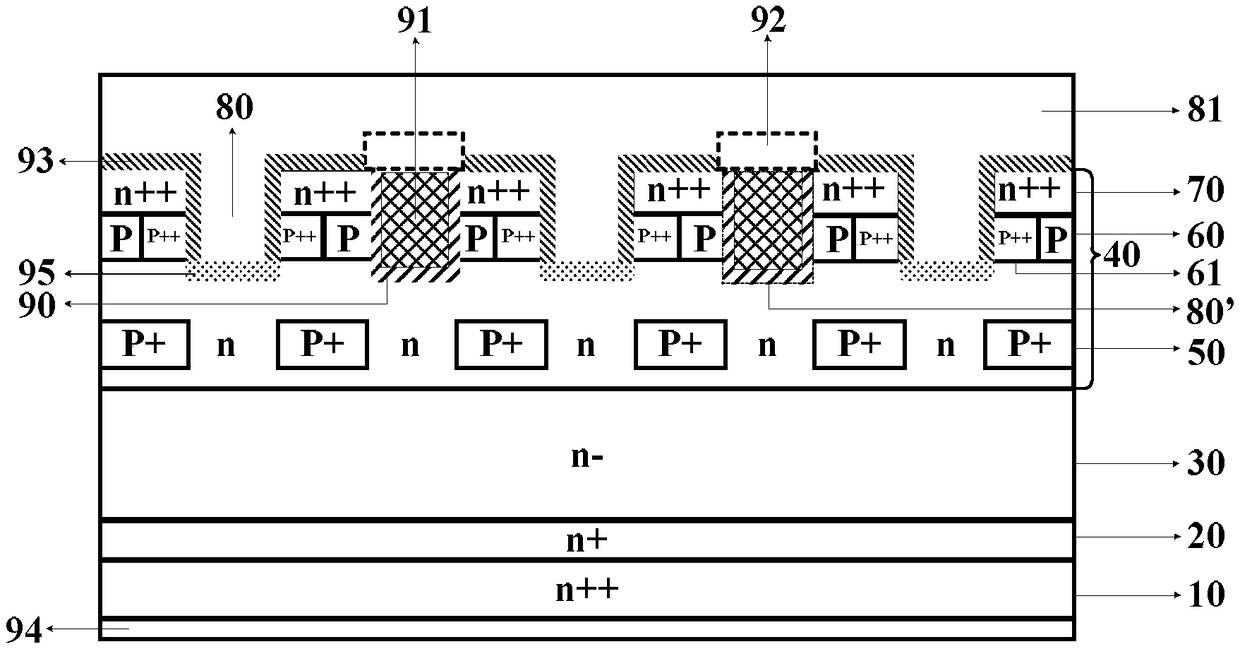
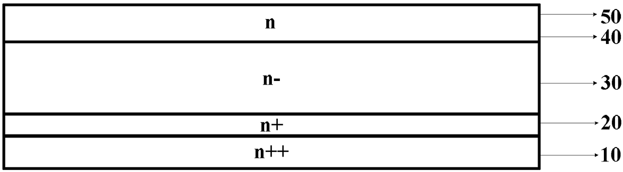
[0047] In one embodiment of the present invention, a structure of a SiC UMOSFET with integrated SBD is provided. figure 1 A schematic structural diagram of the SiC UMOSFET integrated with SBD provided by the present invention is shown, which is the first embodiment of the present invention. like figure 1 As shown, the structure includes: SiC n++ type substrate 10 , n+ buffer layer 20 , n − drift layer 30 , n type current transport layer 40 , p+ type buried layer 50 and active region.

[0048] Each component of the SBD-integrated SiC UMOSFET provided by the present invention will be described in detail below.

[0049] The p+ type buried layer 50 is floating in the n type current transport layer 40 .

[0050] The active ...


PUM

PropertyMeasurementUnit
thicknessaaaaaaaaaa
thicknessaaaaaaaaaa

Abstract

The invention provides a silicon carbide trench gate metal oxide with semiconductor field effect transistor (SiC UMOSFET) structure integrated Schottky diode (SBD) and a method for manufacturing the same, The structure is characterized by, a p +-type bury layer (50) is formed on the n-type current transport layer (40) by implantation, and further an n-type current transport layer (40) is epitaxially formed so that the p +-type buried layer (50) floats, and the p +-type buried layer (50) can effectively reduce the electric field in the gate trench oxide and the electric field at the Schottky contact position in the blocking mode, so that the SBD integrated SiC UMOSFET has high blocking ability, and the high temperature and high field reliability of the device are greatly improved. At that same time, the relative position of the main trench (80), the main trench (80') and the p +-type buried layer (50) and the n-type current transport layer (40) are adjusted so that when the MOSFET is operated in the first quadrant, the conduction characteristic of the MOSFET does not degrade significantly; When the MOSFET is operated in the third quadrant, the conduction of the parasitic pn diode inthe MOSFET is effectively suppressed and the Schottky diode conduction mode is obtained. SiC UMOSFETs with integrated SBD have a lower total chip area than discrete SBD and MOSFET devices.

Description

technical field [0001] The invention relates to a structure and a preparation method of an SBD-integrated SiC UMOSFET, in particular to a structure and a preparation method of a SBD-integrated SiC UMOSFET with a p+ type buried layer. Background technique [0002] SiC has superior physical and electrical properties, such as high critical breakdown electric field, wide band gap, and high electron saturation drift velocity, and is suitable for high-voltage, high-temperature power electronics. Vertical MOS field effect transistors include double injection planar gate type (DMOSFET) and trench gate type (UMOSFET), and 4H-SiC UMOSFET can theoretically have more Small on-resistance and greater channel density, so it has wider application prospects. SiC UMOSFETs are used in some power electronics fields, such as motor drives, inverters, DC-DC conversions, etc., which require their internal parasitic pn-type body diodes to conduct for a period of time. On the one hand, the body dio...

Claims


Application Information

Patent Timeline
Patent Type & Authority Applications(China)
IPC IPC(8): H01L27/07H01L29/06H01L21/82
CPCH01L21/8213H01L27/0727H01L29/0623
Inventor 申占伟张峰闫果果温正欣刘兴昉赵万顺王雷孙国胜曾一平
Owner INST OF SEMICONDUCTORS - CHINESE ACAD OF SCI
Why Eureka
Try Eureka