
A kind of preparation method of light-emitting diode epitaxial wafer and light-emitting diode epitaxial wafer

A technology of light-emitting diodes and epitaxial wafers, applied in semiconductor devices, electrical components, circuits, etc., can solve the problems of low LED luminous efficiency and composite light emission

Active Publication Date: 2020-10-27
HC SEMITEK ZHEJIANG CO LTD
View PDF2 Cites 0 Cited by
  • Summary
  • Abstract
  • Description
  • Claims
  • Application Information

AI Technical Summary

Problems solved by technology

[0006] The embodiment of the present invention provides a method for preparing a light-emitting diode epitaxial wafer and the light-emitting diode epitaxial wafer, which can solve the stress and defects caused by the lattice mismatch between sapphire and gallium nitride in the prior art that affect the electrons and electrons in the active layer. Hole radiation recombination light emission, resulting in low luminous efficiency of LED

Method used


Image

  • A kind of preparation method of light-emitting diode epitaxial wafer and light-emitting diode epitaxial wafer
  • A kind of preparation method of light-emitting diode epitaxial wafer and light-emitting diode epitaxial wafer

Examples


Embodiment Construction

[0028] In order to make the object, technical solution and advantages of the present invention clearer, the implementation manner of the present invention will be further described in detail below in conjunction with the accompanying drawings.

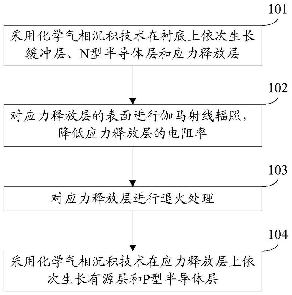
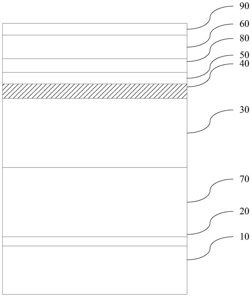
[0029] The embodiment of the present invention provides a method for preparing a light-emitting diode epitaxial wafer, figure 1 For the flow chart of the preparation method of the light-emitting diode epitaxial wafer provided by the embodiment of the present invention, see figure 1 , the preparation method comprises:

[0030] Step 101: sequentially growing a buffer layer, an N-type semiconductor layer and a stress release layer on the substrate by chemical vapor deposition technology.

[0031] Specifically, this step 101 may include:

[0032] Controlling the temperature to 400°C to 600°C (preferably 500°C), the pressure to 400torr to 600torr (preferably 500torr), and growing a buffer layer with a thickness of 15nm to 35nm (preferably...


PUM

PropertyMeasurementUnit
thicknessaaaaaaaaaa
thicknessaaaaaaaaaa
thicknessaaaaaaaaaa

Abstract

The invention discloses a preparation method of a light emitting diode epitaxial wafer and a light emitting diode epitaxial wafer thereof, belonging to the field of semiconductor technology. A manufacture method comprises sequentially grow a buffer layer, an N-type semiconductor layer and a stress release lay on a substrate by a chemical vapor deposition technique; Gamma-ray irradiation is appliedto the surface of the stress-releasing layer to reduce the resistivity of the stress-releasing layer. An active layer and a P-type semiconductor layer were grown on the stress-relief layer by chemical vapor deposition. By irradiating the surface of the stress relief layer with gamma rays, each component of the stress-releasing layer is uniformly doped in the stress-releasing layer, the uniformityand effectiveness of element doping in the stress release layer are improved, Ensuring the consistency and uniformity of the epitaxial wafer growth quality, reducing and releasing the defects and stresses caused by lattice mismatch between sapphire and GaN, and improving the crystal quality of the active layer are conducive to increasing the radiation recombination luminescence in the active layer, and ultimately improving the luminescence efficiency of the LED.

Description

technical field [0001] The invention relates to the technical field of semiconductors, in particular to a method for preparing a light-emitting diode epitaxial wafer and the light-emitting diode epitaxial wafer. Background technique [0002] A light-emitting diode (English: Light Emitting Diode, referred to as: LED) is a semiconductor electronic component that can emit light. LED has attracted wide attention due to its advantages of energy saving, environmental protection, high reliability, and long service life. For civil lighting, luminous efficiency and service life are the main criteria, so increasing the luminous efficiency of LEDs and improving the antistatic ability of LEDs is particularly critical for the wide application of LEDs. [0003] Epitaxial wafers are the primary products in the LED manufacturing process. The existing LED epitaxial wafer includes a substrate, a buffer layer, an N-type semiconductor layer, an active layer and a P-type semiconductor layer, a...

Claims


Application Information

Patent Timeline
Patent Type & Authority Patents(China)
IPC IPC(8): H01L33/12H01L33/00
CPCH01L33/0066H01L33/0075H01L33/0095H01L33/12
Inventor 王群郭炳磊葛永晖董彬忠李鹏王江波
Owner HC SEMITEK ZHEJIANG CO LTD
Learn More