A passivation method for improving high and low temperature stability of SiC MOSFET Devices

A stable and low-temperature technology, applied in the fields of semiconductor devices, semiconductor/solid-state device manufacturing, electrical components, etc., can solve the problems of not considering the temperature and the impact without specifying the evaluation, and achieve the effect of reducing the impact and improving the stability.

Inactive Publication Date: 2018-12-28
DALIAN UNIV OF TECH
View PDF12 Cites 4 Cited by
  • Summary
  • Abstract
  • Description
  • Claims
  • Application Information

AI Technical Summary

Problems solved by technology

However, the patent applicant did not consider the effect of temperature on i

Method used


Image

  • A passivation method for improving high and low temperature stability of SiC MOSFET Devices
  • A passivation method for improving high and low temperature stability of SiC MOSFET Devices
  • A passivation method for improving high and low temperature stability of SiC MOSFET Devices

Examples


Embodiment 1

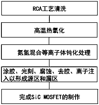
[0031] Such as figure 1 As shown, a passivation method for improving high and low temperature stability of SiC MOSFET devices includes the following steps:

[0032] Step 1, using RCA process cleaning, specifically including the following sub-steps:

[0033] (a) Place the silicon carbide wafer in a mixed solution of concentrated sulfuric acid and hydrogen peroxide, wash it at 100°C for 30 minutes, and rinse the surface of the silicon carbide wafer several times with deionized water. The volume ratio of the concentrated sulfuric acid and hydrogen peroxide is 1:1 ;

[0034] (b) Take out the silicon carbide wafer in sub-step (a) and place it in No. 1 cleaning solution, wash it at 80°C for 10 minutes, then wash it with a hydrofluoric acid aqueous solution with a concentration of 1%, and rinse the surface of the silicon carbide wafer with deionized water Several times, the No. 1 cleaning solution is a mixed solution composed of water, hydrogen peroxide and ammonia in a volume rati...

Embodiment 2

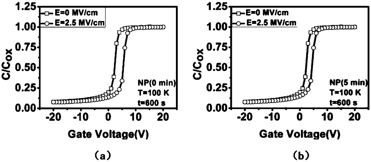
[0045] Low-temperature and high-frequency C-V curve tests were performed on SiC MOS devices that were not treated and treated with nitrogen plasma for 5 minutes. High frequency C-V curves were measured immediately again in situ. The measured results are as figure 2 As shown, wherein: (a) is the C-V drift curve of the sample without passivation treatment, and the flat-band voltage drift value at low temperature 100K is 3.14V (the flat-band voltage extracted from the C-V curve after normal stress and the mean extracted from the C-V curve before stress The difference of the belt voltage), the middle belt voltage drift value is 2.78V (the difference between the middle belt voltage extracted from the C-V curve after the normal stress and the middle belt voltage extracted from the C-V curve before the stress), and figure 2 (b) is the C-V drift curve of the sample treated with nitrogen plasma passivation for 5 minutes. The low-temperature 100K flat-band voltage drift value is 2.87...

Embodiment 3

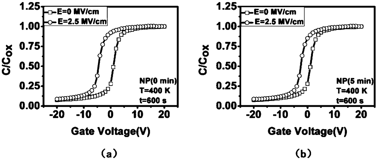
[0047] High-temperature and high-frequency C-V curve tests were performed on SiC MOS devices that were not treated and treated with nitrogen plasma for 5 minutes. High frequency C-V curves were measured immediately again in situ. The measured results are as image 3 As shown, where: (a) is the C-V drift curve of the sample without passivation treatment, the flat-band voltage drift value of the high temperature 400K is -7.25V, (b) is the C-V drift curve of the sample treated with nitrogen plasma passivation for 5 minutes , the high temperature 400K flat-band voltage drift value is -5.39V. Table 1 and Table 2 respectively show the flat-band voltage drift value and middle-band voltage drift value of SiC MOS samples with different nitrogen plasma passivation treatment times under normal stress when measured at 100K and 400K, and the middle-band voltage drift value under high temperature test The effect of other traps and charges cannot be calculated. It can be seen from the two...


PUM


Abstract

The invention relates to the technical field of manufacture and reliability of silicon carbide semiconductor devices and provides a passivation method for improving high and low temperature stabilityof SiC MOSFET devices comprises the following steps: (1) performing cleaning by an RCA process; (2) performing high temperature thermal oxidation; (3) performing nitrogen-hydrogen mixed plasma passivation treatment; (4) performing glue coating, photolithography, etching, glue removing, and ion implantation to form a source region and a drain region, and (5) manufacturing the SiC MOSFET. The methodhas the advantages that N-H in the nitrogen-hydrogen mixed plasma effectively passivates the oxide trap and the interface trap, in which the H element can passivate oxide traps and interface traps onthe basis of N passivation, and the deep-level traps generated by excess nitrogen are moved to the lower half of the forbidden band or beyond the forbidden band, which reduces the influence of trapson the stability of the MOSFET and improves the stability of SiC MOSFET at low temperature (80-300K) and high temperature (300-500K).

Description

technical field [0001] The invention relates to a passivation method for improving the high and low temperature stability of SiC MOSFET devices, and belongs to the technical field of silicon carbide semiconductor device manufacturing and reliability. Background technique [0002] SiC semiconductors are widely used in harsh environments such as high temperature, high frequency and high voltage because of their advantages such as high carrier drift speed, large bandgap width, and strong critical breakdown electric field, and because SiC semiconductors are the only ones that can directly heat Oxidation to form SiO 2 Thin-film wide bandgap compound semiconductor, so it can replace traditional silicon to manufacture SiC MOS devices. However, in the actual oxidation and subsequent steps, the excellent performance of the SiC MOS device will be deteriorated. The macroscopic manifestation in the SiC MOS device is a serious drift in the flat band voltage (MOSFET threshold voltage) of...

Claims


Application Information

Patent Timeline
IPC IPC(8): H01L21/04H01L29/78
CPCH01L21/045H01L29/66068H01L29/78
Inventor 王德君孙雨浓杨超秦福文
Owner DALIAN UNIV OF TECH
Why Eureka
Try Eureka